ZHCSEL0D February   2016  – October 2021 TCAN1042-Q1 , TCAN1042G-Q1 , TCAN1042GV-Q1 , TCAN1042H-Q1 , TCAN1042HG-Q1 , TCAN1042HGV-Q1 , TCAN1042HV-Q1 , TCAN1042V-Q1

PRODUCTION DATA  

  1. 特性
  2. 应用
  3. 说明
  4. Revision History
  5. Device Comparison Table
  6. Pin Configurations and Functions
  7. Specifications
    1. 7.1 Absolute Maximum Ratings
    2. 7.2 ESD Ratings
    3. 7.3 ESD Ratings, Specifications
    4. 7.4 Recommended Operating Conditions
    5. 7.5 Thermal Information
    6. 7.6 Power Rating
    7. 7.7 Electrical Characteristics
    8. 7.8 Switching Characteristics
    9. 7.9 Typical Characteristics
  8. Parameter Measurement Information
  9. Detailed Description
    1. 9.1 Overview
    2. 9.2 Functional Block Diagram
    3. 9.3 Feature Description
      1. 9.3.1 TXD Dominant Timeout (DTO)
      2. 9.3.2 Thermal Shutdown (TSD)
      3. 9.3.3 Undervoltage Lockout
      4. 9.3.4 Unpowered Device
      5. 9.3.5 Floating Terminals
      6. 9.3.6 CAN Bus Short Circuit Current Limiting
      7. 9.3.7 Digital Inputs and Outputs
        1. 9.3.7.1 Devices with VCC Only (Devices without the "V" Suffix):
        2. 9.3.7.2 Devices with VIO I/O Level Shifting (Devices with "V" Suffix):
    4. 9.4 Device Functional Modes
      1. 9.4.1 CAN Bus States
      2. 9.4.2 Normal Mode
      3. 9.4.3 Standby Mode
        1. 9.4.3.1 Remote Wake Request via Wake Up Pattern (WUP) in Standby Mode
      4. 9.4.4 Driver and Receiver Function Tables
  10. 10Application Information Disclaimer
    1. 10.1 Application Information
    2. 10.2 Typical Applications
      1. 10.2.1 Design Requirements
        1. 10.2.1.1 Bus Loading, Length and Number of Nodes
      2. 10.2.2 Detailed Design Procedures
        1. 10.2.2.1 CAN Termination
      3. 10.2.3 Application Curves
  11. 11Power Supply Recommendations
  12. 12Device and Documentation Support
    1. 12.1 接收文档更新通知
    2. 12.2 支持资源
    3. 12.3 Trademarks
    4. 12.4 Electrostatic Discharge Caution
    5. 12.5 术语表
  13. 13Mechanical, Packaging, and Orderable Information

封装选项

请参考 PDF 数据表获取器件具体的封装图。

机械数据 (封装 | 引脚)
  • D|8
  • DRB|8
散热焊盘机械数据 (封装 | 引脚)
订购信息

CAN Bus States

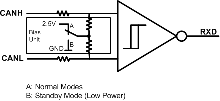
The CAN bus has two states during powered operation of the device: dominant and recessive. A dominant bus state is when the bus is driven differentially, corresponding to a logic low on the TXD and RXD terminal. A recessive bus state is when the bus is biased to VCC / 2 via the high-resistance internal input resistors RIN of the receiver, corresponding to a logic high on the TXD and RXD terminals.
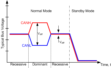
GUID-A4DF0427-AC58-44A9-A0F3-AA72823F26D8-low.pngFigure 9-2 Bus States (Physical Bit Representation)
GUID-CE9B5DD5-F389-4175-9D0D-89BC427F6045-low.pngFigure 9-3 Bias Unit (Recessive Common Mode Bias) and Receiver