ZHCSN78E january   2021  – march 2023 TCAN1043A-Q1

PRODUCTION DATA  

  1. 特性
  2. 应用
  3. 说明
  4. Revision History
  5. Pin Configuration and Functions
  6. Specifications
    1. 6.1  Absolute Maximum Ratings
    2. 6.2  ESD Ratings
    3. 6.3  ESD Ratings - IEC Specifications
    4. 6.4  Recommended Operating Conditions
    5. 6.5  Thermal Information
    6. 6.6  Power Dissipation Ratings
    7. 6.7  Power Supply Characteristics
    8. 6.8  Electrical Characteristics
    9. 6.9  Timing Requirements
    10. 6.10 Switching Characteristics
    11. 6.11 Typical Characteristics
  7. Parameter Measurement Information
  8. Detailed Description
    1. 8.1 Overview
    2. 8.2 Functional Block Diagram
    3. 8.3 Feature Description
      1. 8.3.1 Supply Pins
        1. 8.3.1.1 VSUP Pin
        2. 8.3.1.2 VCC Pin
        3. 8.3.1.3 VIO Pin
      2. 8.3.2 Digital Inputs and Outputs
        1. 8.3.2.1 TXD Pin
        2. 8.3.2.2 RXD Pin
        3. 8.3.2.3 nFAULT Pin
        4. 8.3.2.4 EN Pin
        5. 8.3.2.5 nSTB Pin
      3. 8.3.3 GND
      4. 8.3.4 INH Pin
      5. 8.3.5 WAKE Pin
      6. 8.3.6 CAN Bus Pins
      7. 8.3.7 Faults
        1. 8.3.7.1 Internal and External Fault Indicators
          1. 8.3.7.1.1 Power-Up (PWRON Flag)
          2. 8.3.7.1.2 Wake-Up Request (WAKERQ Flag)
          3. 8.3.7.1.3 Undervoltage Faults
            1. 8.3.7.1.3.1 Undervoltage on VSUP
            2. 8.3.7.1.3.2 Undervoltage on VCC
            3. 8.3.7.1.3.3 Undervoltage on VIO
          4. 8.3.7.1.4 CAN Bus Fault (CBF Flag)
          5. 8.3.7.1.5 TXD Clamped Low (TXDCLP Flag)
          6. 8.3.7.1.6 TXD Dominant State Timeout (TXDDTO Flag)
          7. 8.3.7.1.7 TXD Shorted to RXD Fault (TXDRXD Flag)
          8. 8.3.7.1.8 CAN Bus Dominant Fault (CANDOM Flag)
      8. 8.3.8 Local Faults
        1. 8.3.8.1 TXD Clamped Low (TXDCLP)
        2. 8.3.8.2 TXD Dominant Timeout (TXD DTO)
        3. 8.3.8.3 Thermal Shutdown (TSD)
        4. 8.3.8.4 Undervoltage Lockout (UVLO)
        5. 8.3.8.5 Unpowered Devices
        6. 8.3.8.6 Floating Terminals
        7. 8.3.8.7 CAN Bus Short-Circuit Current Limiting
    4. 8.4 Device Functional Modes
      1. 8.4.1 Operating Mode Description
        1. 8.4.1.1 Normal Mode
        2. 8.4.1.2 Silent Mode
        3. 8.4.1.3 Standby Mode
        4. 8.4.1.4 Go-To-Sleep Mode
        5. 8.4.1.5 Sleep Mode
          1. 8.4.1.5.1 Remote Wake Request via Wake-Up Pattern (WUP)
          2. 8.4.1.5.2 Local Wake-Up (LWU) via WAKE Input Terminal
      2. 8.4.2 CAN Transceiver
        1. 8.4.2.1 CAN Transceiver Operation
          1. 8.4.2.1.1 CAN Transceiver Modes
            1. 8.4.2.1.1.1 CAN Off Mode
            2. 8.4.2.1.1.2 CAN Autonomous: Inactive and Active
            3. 8.4.2.1.1.3 CAN Active
          2. 8.4.2.1.2 Driver and Receiver Function Tables
          3. 8.4.2.1.3 CAN Bus States
  9. Application Information Disclaimer
    1. 9.1 Application Information
      1. 9.1.1 Typical Application
      2. 9.1.2 Design Requirements
        1. 9.1.2.1 Bus Loading, Length and Number of Nodes
      3. 9.1.3 Detailed Design Procedure
        1. 9.1.3.1 CAN Termination
    2. 9.2 Application Curves
  10. 10Power Supply Recommendations
  11. 11Layout
    1. 11.1 Layout Guidelines
    2. 11.2 Layout Example
  12. 12Device and Documentation Support
    1. 12.1 Documentation Support
    2. 12.2 接收文档更新通知
    3. 12.3 支持资源
    4. 12.4 商标
    5. 12.5 静电放电警告
    6. 12.6 术语表
  13. 13Mechanical, Packaging, and Orderable Information

封装选项

机械数据 (封装 | 引脚)
散热焊盘机械数据 (封装 | 引脚)
订购信息

CAN Termination

Termination may be a single 120-Ω resistor at each end of the bus, either on the cable or in a terminating node. If filtering and stabilization of the common-mode voltage of the bus is desired then split termination may be used, see Figure 9-2. Split termination improves the electromagnetic emissions behavior of the network by filtering higher-frequency common-mode noise that may be present on the differential signal lines.
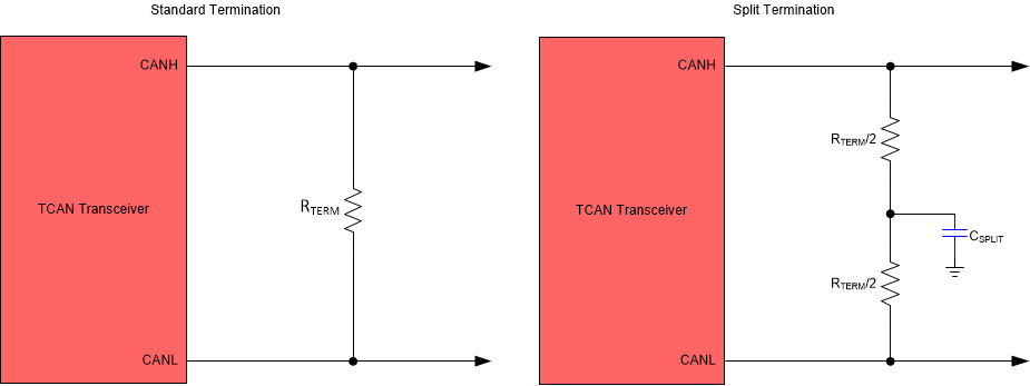
GUID-52BC5CDD-EC14-4D7E-881B-887C9CB6FDD3-low.gifFigure 9-2 CAN Bus Termination Concepts