ZHCSO46 December   2021 TCAN1057AEV-Q1

PRODUCTION DATA  

  1. 特性
  2. 应用
  3. 说明
  4. Revision History
  5. Pin Configuration and Functions
  6. Specifications
    1. 6.1 Absolute Maximum Ratings
    2. 6.2 ESD Ratings
    3. 6.3 ESD Ratings Table — IEC Specifications
    4. 6.4 Recommended Operating Conditions
    5. 6.5 Thermal Characteristics
    6. 6.6 Supply Characteristics
    7. 6.7 Dissipation Ratings
    8. 6.8 Electrical Characteristics
    9. 6.9 Switching Characteristics
  7. Parameter Measurement Information
  8. Detailed Description
    1. 8.1 Overview
    2. 8.2 Functional Block Diagram
    3. 8.3 Feature Description
      1. 8.3.1 Pin Description
        1. 8.3.1.1 TXD
        2. 8.3.1.2 GND
        3. 8.3.1.3 VCC
        4. 8.3.1.4 RXD
        5. 8.3.1.5 VIO
        6. 8.3.1.6 CANH and CANL
        7. 8.3.1.7 S (Silent)
      2. 8.3.2 CAN Bus States
      3. 8.3.3 TXD Dominant Timeout (DTO)
      4. 8.3.4 CAN Bus Short-Circuit Current Limiting
      5. 8.3.5 Thermal Shutdown (TSD)
      6. 8.3.6 Undervoltage Lockout
      7. 8.3.7 Unpowered Device
      8. 8.3.8 Floating Pins
    4. 8.4 Device Functional Modes
      1. 8.4.1 Operating Modes
      2. 8.4.2 Normal Mode
      3. 8.4.3 Silent Mode
      4. 8.4.4 Driver and Receiver Function
  9. Application and Implementation
    1. 9.1 Application Information
    2. 9.2 Typical Application
      1. 9.2.1 Design Requirements
        1. 9.2.1.1 CAN Termination
      2. 9.2.2 Detailed Design Procedures
        1. 9.2.2.1 Bus Loading, Length and Number of Nodes
      3. 9.2.3 Application Curves
      4. 9.2.4 System Examples
  10. 10Power Supply Recommendations
  11. 11Layout
    1. 11.1 Layout Guidelines
    2. 11.2 Layout Example
  12. 12Device and Documentation Support
    1. 12.1 Documentation Support
    2. 12.2 接收文档更新通知
    3. 12.3 支持资源
    4. 12.4 Trademarks
    5. 12.5 Electrostatic Discharge Caution
    6. 12.6 术语表
  13. 13Mechanical, Packaging, and Orderable Information

封装选项

机械数据 (封装 | 引脚)
散热焊盘机械数据 (封装 | 引脚)
订购信息

CAN Bus States

The CAN bus has two logical states during operation: recessive and dominant. See Figure 8-1.

A dominant bus state occurs when the bus is driven differentially and corresponds to a logic low on the TXD and RXD pins. A recessive bus state occurs when the bus is biased to VCC/2 through the high-resistance internal input resistors (RIN) of the receiver and corresponds to a logic high on the TXD and RXD pins.

A dominant state overwrites the recessive state during arbitration. Multiple CAN nodes can transmit a dominant bit at the same time during arbitration, and in this case the differential voltage of the bus is greater than the differential voltage of a single driver.
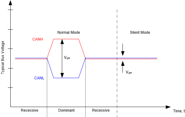
GUID-84DAC41F-569C-4234-BD11-A494FCB3A741-low.gifFigure 8-1 Bus States