ZHCSPG0 December 2021 TCAN1167-Q1
PRODUCTION DATA
- 1 特性
- 2 应用
- 3 说明
- 4 Revision History
- 5 说明(续)
- 6 Pin Configurations and Functions
- 7 Specifications
- 8 Parameter Measurement Information
-
9 Detailed Description
- 9.1 Overview
- 9.2 Functional Block Diagram
- 9.3
Feature Description
- 9.3.1 VSUP Pin
- 9.3.2 VCCOUT Pin
- 9.3.3 Digital Inputs and Outputs
- 9.3.4 GND
- 9.3.5 INH Pin
- 9.3.6 WAKE Pin
- 9.3.7 nRST Pin
- 9.3.8 SDO
- 9.3.9 nCS Pin
- 9.3.10 SCLK
- 9.3.11 SDI
- 9.3.12 CAN Bus Pins
- 9.3.13 Local Faults
- 9.3.14 Watchdog
- 9.3.15 Bus Fault Detection and Communication
- 9.4 Device Functional Modes
- 9.5
Programming
- 9.5.1 Serial Peripheral Interface (SPI) Communication
- 9.5.2 Serial Clock Input (SCLK)
- 9.5.3 Serial Data Input (SDI)
- 9.5.4 Serial Data Output (SDO)
- 9.5.5 Chip Select Not (nCS)
- 9.5.6
Registers
- 9.5.6.1 DEVICE_ID_y Register (Address = 0h + formula) [reset = xxh]
- 9.5.6.2 REV_ID_MAJOR Register (Address = 8h) [reset = 00h]
- 9.5.6.3 REV_ID_MINOR Register (Address = 9h) [reset = 00h]
- 9.5.6.4 SPI_RSVD_x Register (Address = Ah + formula) [reset = 00h]
- 9.5.6.5 Scratch_Pad_SPI Register (Address = Fh) [reset = 00h]
- 9.5.6.6 MODE_CNTRL Register (Address = 10h) [reset = 04h]
- 9.5.6.7 WD_CONFIG_1 Register (Address = 13h) [reset = 54h]
- 9.5.6.8 WD_CONFIG_2 Register (Address = 14h) [reset = 02h]
- 9.5.6.9 WD_INPUT_TRIG Register (Address = 15h) [reset = 00h]
- 9.5.6.10 WD_QA_CONFIG Register (Address = 2Dh) [reset = 0h]
- 9.5.6.11 WD_QA_ANSWER Register (Address = 2Eh) [reset = 0h]
- 9.5.6.12 WD_QA_QUESTION Register (Address = 2Fh) [reset = 0h]
- 9.5.6.13 STATUS (address = 40h) [reset = 00h]
- 9.5.6.14 INT_GLOBAL Register (Address = 50h) [reset = 0h]
- 9.5.6.15 INT_1 Register (Address = 51h) [reset = 0h]
- 9.5.6.16 INT_2 Register (Address = 52h) [reset = 40h]
- 9.5.6.17 INT_3 Register (Address 53h) [reset = 0h]
- 9.5.6.18 INT_CANBUS Register (Address = 54h) [reset = 0h]
- 9.5.6.19 INT_ENABLE_1 Register (Address = 56h) [reset = F3h]
- 9.5.6.20 INT_ENABLE_2 Register (Address = 57h) [reset = 3Fh]
- 9.5.6.21 INT_ENABLE_3 Register (Address =58h) [reset = 80h]
- 9.5.6.22 INT_ENABLE_CANBUS Register (Address = 59h) [reset = 7Fh]
- 9.5.6.23 INT_RSVD_y Register (Address = 5Ah + formula) [reset = 00h]
- 10Application Information Disclaimer
- 11Power Supply Requirements
- 12Layout
- 13Device and Documentation Support
- 14Mechanical, Packaging, and Orderable Information
9.4.2.4 CAN Bus States
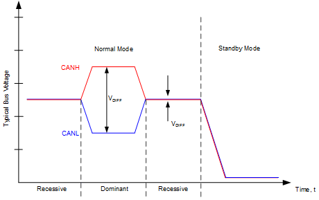
The CAN bus has two logical states during operation: recessive and dominant. See Figure 9-20.
A dominant bus state occurs when the bus is driven differentially and corresponds to a logic low on the TXD and RXD pins. A recessive bus state occurs when the bus is biased to one half of the CAN transceiver supply voltage via the high resistance internal input resistors (RIN) of the receiver and corresponds to a logic high on the TXD and RXD pins.
A dominant state overwrites the recessive state during arbitration. Multiple CAN nodes may be transmitting a dominant bit at the same time during arbitration, and in this case the differential voltage of the CAN bus will be greater than the differential voltage of a single CAN driver. The TCAN1167-Q1 CAN transceiver implements low-power standby and sleep modes which enables a third bus state where the bus pins are biased to ground via the high resistance internal resistors of the receiver.
 Figure 9-20 Bus States