ZHCSEG6E December 2015 – December 2019 TCAN330 , TCAN330G , TCAN332 , TCAN332G , TCAN334 , TCAN334G , TCAN337 , TCAN337G
PRODUCTION DATA.
- 1 特性
- 2 应用
- 3 说明
- 4 修订历史记录
- 5 说明 (续)
- 6 Device Options
- 7 Pin Configuration and Functions
- 8 Specifications
- 9 Parameter Measurement Information
- 10Detailed Description
- 11Application and Implementation
- 12Power Supply Recommendations
- 13Layout
- 14器件和文档支持
- 15机械、封装和可订购信息
封装选项
机械数据 (封装 | 引脚)
散热焊盘机械数据 (封装 | 引脚)
- DCN|8
订购信息
10.4.1 CAN Bus States
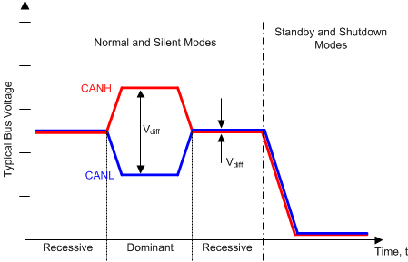
The CAN bus has two logical states during operation: recessive and dominant. See Figure 31 and Figure 32.
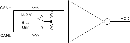
Recessive bus state is when the high resistive internal input resistors of each node's receiver bias the bus to a common mode of about 1.85 V across the bus termination resistors. Recessive is equivalent to logic high and is typically a differential voltage on the bus of about 0 V. Recessive state is also the idle state.
Dominant bus state is when the bus is driven differentially by one or more drivers. Current is induced to flow through the termination resistors and generate a differential voltage on the bus. Dominant is equivalent to logic low and is a differential voltage on the bus greater than the minimum threshold for a CAN dominant. A dominant state overwrites the recessive state.
During arbitration, multiple CAN nodes may transmit a dominant bit at the same time. In this case the differential voltage of the bus will be greater than the differential voltage of a single driver.
The host microprocessor of the CAN node will use the TXD terminal to drive the bus and will receive data from the bus on the RXD pin.
Transceivers with low power Standby Mode have a third bus state where the bus terminals are weakly biased to ground via the high resistance internal resistors of the receiver. See Figure 31 and Figure 32.
 Figure 31. Bus States (Physical Bit Representation) Figure 31. Bus States (Physical Bit Representation) |

A. Normal and Silent Modes
B. Standby and Shutdown Modes Figure 32. Simplified Recessive Common Mode Bias Unit and Receiver |
The devices have four main operating modes:
- Normal mode (all devices)
- Silent mode (TCAN330, TCAN337)
- Standby mode with wake (TCAN334)
- Shutdown mode (TCAN330, TCAN334)
Table 3. CAN Transceivers with Silent Mode
| S | Device MODE | DRIVER | RECEIVER | RXD PIN |
|---|---|---|---|---|
| HIGH | Reduced Power Silent (Listen) Mode | Disabled (OFF)(2) | Enabled (ON) | Mirrors Bus State(1) |
| LOW/NC | Normal Mode | Enabled (ON) | Enabled (ON) |
Table 4. CAN Transceivers with Standby Mode with Wake
| STB | Device MODE | DRIVER | RECEIVER | RXD Terminal |
|---|---|---|---|---|
| HIGH | Ultra Low Current Standby Mode | Disabled (OFF)(2) | Low Power Receiver and Bus Monitor Enabled (ON) | High (Recessive) until WUP, then filtered mirrors of Bus State (1) |
| LOW/NC | Normal Mode | Enabled (ON) | Enabled (ON) | Mirrors Bus State (1) |