ZHCSEG6E December   2015  – December 2019 TCAN330 , TCAN330G , TCAN332 , TCAN332G , TCAN334 , TCAN334G , TCAN337 , TCAN337G

PRODUCTION DATA.  

  1. 特性
  2. 应用
  3. 说明
    1.     方框图
  4. 修订历史记录
  5. 说明 (续)
  6. Device Options
  7. Pin Configuration and Functions
    1.     Pin Functions
  8. Specifications
    1. 8.1 Absolute Maximum Ratings
    2. 8.2 ESD Ratings
    3. 8.3 Recommended Operating Conditions
    4. 8.4 Thermal Information
    5. 8.5 Electrical Characteristics
    6. 8.6 Switching Characteristics
    7. 8.7 Typical Characteristics
    8. 8.8 Typical Characteristics, TCAN330 Receiver
    9. 8.9 Typical Characteristics, TCAN330 Driver
  9. Parameter Measurement Information
  10. 10Detailed Description
    1. 10.1 Overview
    2. 10.2 Functional Block Diagram
    3. 10.3 Feature Description
      1. 10.3.1 TXD Dominant Timeout (TXD DTO)
      2. 10.3.2 RXD Dominant Timeout (RXD DTO)
      3. 10.3.3 Thermal Shutdown
      4. 10.3.4 Undervoltage Lockout and Unpowered Device
      5. 10.3.5 Fault Pin (TCAN337)
      6. 10.3.6 Floating Pins
      7. 10.3.7 CAN Bus Short Circuit Current Limiting
      8. 10.3.8 ESD Protection
      9. 10.3.9 Digital Inputs and Outputs
    4. 10.4 Device Functional Modes
      1. 10.4.1 CAN Bus States
      2. 10.4.2 Normal Mode
      3. 10.4.3 Silent Mode
      4. 10.4.4 Standby Mode with Wake
      5. 10.4.5 Bus Wake via RXD Request (BWRR) in Standby Mode
      6. 10.4.6 Shutdown Mode
      7. 10.4.7 Driver and Receiver Function Tables
  11. 11Application and Implementation
    1. 11.1 Application Information
      1. 11.1.1 Bus Loading, Length and Number of Nodes
    2. 11.2 Typical Application
      1. 11.2.1 Design Requirements
        1. 11.2.1.1 CAN Termination
      2. 11.2.2 Detailed Design Procedure
      3. 11.2.3 Application Curves
    3. 11.3 System Examples
      1. 11.3.1 ISO11898 Compliance of TCAN33x Family of 3.3-V CAN Transceivers Introduction
      2. 11.3.2 Differential Signal
      3. 11.3.3 Common-Mode Signal and EMC Performance
  12. 12Power Supply Recommendations
  13. 13Layout
    1. 13.1 Layout Guidelines
    2. 13.2 Layout Example
  14. 14器件和文档支持
    1. 14.1 相关链接
    2. 14.2 支持资源
    3. 14.3 商标
    4. 14.4 静电放电警告
    5. 14.5 Glossary
  15. 15机械、封装和可订购信息

封装选项

机械数据 (封装 | 引脚)
散热焊盘机械数据 (封装 | 引脚)
订购信息

Parameter Measurement Information

TCAN330 TCAN332 TCAN334 TCAN337 TCAN330G TCAN332G TCAN334G TCAN337G Supply_Test_Circuit_sllseq7.gifFigure 18. Supply Test Circuit
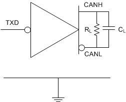
TCAN330 TCAN332 TCAN334 TCAN337 TCAN330G TCAN332G TCAN334G TCAN337G Driver_Test_Circuit_sllseq7.gifFigure 19. Driver Test Circuit and Measurement
TCAN330 TCAN332 TCAN334 TCAN337 TCAN330G TCAN332G TCAN334G TCAN337G Receiver_Test_Circuit_sllseq7.gifFigure 20. Receiver Test Circuit and Measurement
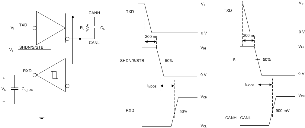
TCAN330 TCAN332 TCAN334 TCAN337 TCAN330G TCAN332G TCAN334G TCAN337G tMODE_from_SHDN_S_STB_sllseq7.gifFigure 21. tMODE Test Circuit and Measurement, from Normal to Shutdown, Standby or Silent Mode
TCAN330 TCAN332 TCAN334 TCAN337 TCAN330G TCAN332G TCAN334G TCAN337G tMODE_to_SHDN_S_STB_sllseq7.gifFigure 22. tMODE Test Circuit and Measurement, from Shutdown, Standby or Silent to Normal Mode
TCAN330 TCAN332 TCAN334 TCAN337 TCAN330G TCAN332G TCAN334G TCAN337G TPROP(LOOP)_sllseq7.gifFigure 23. tPROP(LOOP) Test Circuit and Measurement
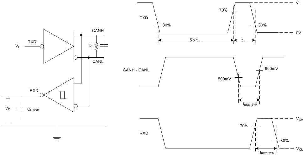
TCAN330 TCAN332 TCAN334 TCAN337 TCAN330G TCAN332G TCAN334G TCAN337G Loop_Delay_Symmetry_sllseq7.gifFigure 24. Loop Delay Symmetry Test Circuit and Measurement
TCAN330 TCAN332 TCAN334 TCAN337 TCAN330G TCAN332G TCAN334G TCAN337G TXD_DTO_Circuit_sllseq7.gifFigure 25. TXD Dominant Time Out Test Circuit and Measurement
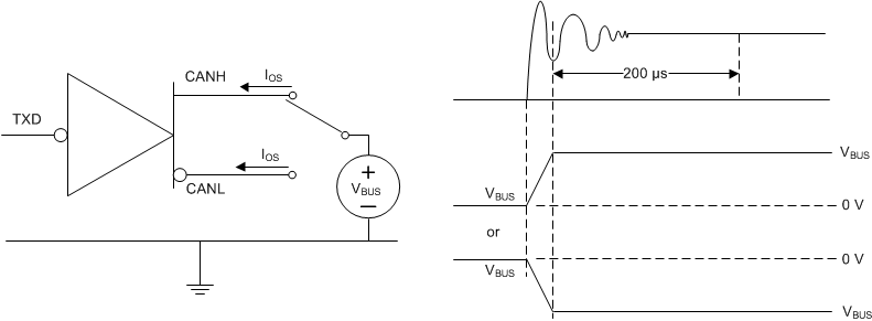
TCAN330 TCAN332 TCAN334 TCAN337 TCAN330G TCAN332G TCAN334G TCAN337G Driver_Short_Circuit_sllseq7.gifFigure 26. Driver Short-Circuit Current Test and Measurement
TCAN330 TCAN332 TCAN334 TCAN337 TCAN330G TCAN332G TCAN334G TCAN337G RXD_DTO_Circuit_sllseq7.gifFigure 27. RXD Dominant Timeout Test Circuit and Measurement
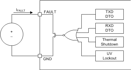
TCAN330 TCAN332 TCAN334 TCAN337 TCAN330G TCAN332G TCAN334G TCAN337G FAULT_Test_sllseq7.gifFigure 28. FAULT Test and Measurement