ZHCSH93 December   2017 TCAN4420

PRODUCTION DATA.  

  1. 特性
  2. 应用
  3. 说明
    1.     Device Images
      1.      功能框图
  4. 修订历史记录
  5. Pin Configuration and Functions
    1.     Pin Functions
  6. Specifications
    1. 6.1 Absolute Maximum Ratings
    2. 6.2 ESD Ratings
    3. 6.3 ESD Ratings Specifications
    4. 6.4 Recommended Operating Conditions
    5. 6.5 Thermal Information
    6. 6.6 Power Supply Characteristics
    7. 6.7 AC and DC Electrical Characteristics
    8. 6.8 Timing Requirements
    9. 6.9 Typical Characteristics
  7. Parameter Measurement Information
  8. Detailed Description
    1. 8.1 Overview
    2. 8.2 Functional Block Diagrams
    3. 8.3 Feature Description
      1. 8.3.1 TXD Dominant Time Out (DTO)
      2. 8.3.2 CAN Bus Short Circuit Current Limiting
      3. 8.3.3 Thermal Shutdown
      4. 8.3.4 Under Voltage Lockout (UVLO) and Unpowered Device
        1. 8.3.4.1 VIO Supply PIN
    4. 8.4 Device Functional Modes
      1. 8.4.1 Polarity Configuration
      2. 8.4.2 Normal Polarity Mode
      3. 8.4.3 Reverse Polarity Mode
      4. 8.4.4 Driver and Receiver Function
      5. 8.4.5 Floating Terminals
  9. Application and Implementation
    1. 9.1 Application Information
    2. 9.2 Typical Application
      1. 9.2.1 Design Requirements
        1. 9.2.1.1 Bus Loading, Length and Number of Nodes
      2. 9.2.2 Detailed Design Procedure
        1. 9.2.2.1 CAN Termination
      3. 9.2.3 Application Curves
  10. 10Power Supply Recommendations
  11. 11Layout
    1. 11.1 Layout Guidelines
    2. 11.2 Layout Example
  12. 12器件和文档支持
    1. 12.1 器件支持
      1. 12.1.1 器件命名规则
    2. 12.2 接收文档更新通知
    3. 12.3 社区资源
    4. 12.4 商标
    5. 12.5 静电放电警告
    6. 12.6 Glossary
  13. 13机械、封装和可订购信息

封装选项

请参考 PDF 数据表获取器件具体的封装图。

机械数据 (封装 | 引脚)
  • D|8
散热焊盘机械数据 (封装 | 引脚)
订购信息

Pin Configuration and Functions

D Package
8-Pin SOIC
Top View
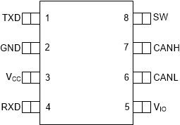
TCAN4420 Pinout_D_TCAN4420.gif

Pin Functions

PIN I/O DESCRIPTION
NAME NO.
TXD 1 Logic Input CAN transmit data input (LOW for dominant and HIGH for recessive bus states)
GND 2 Ground Ground connection
VCC 3 Power 5 V ±10% supply voltage
RXD 4 Logic Output CAN receive data output (LOW for dominant and HIGH for recessive bus states)
VIO 5 Power Transceiver I/O level shifting supply voltage
CANL 6 Bus I/O Low level CAN bus input/output line
CANH 7 Bus I/O High level CAN bus input/output line
SW 8 Logic Input Polarity switch pin. Set to low for normal polarity (default), and high to reverse the polarity of the CAN pins