ZHCSJ74A December 2018 – January 2020 TCAN4550
PRODUCTION DATA.
- 1 特性
- 2 应用
- 3 说明
- 4 修订历史记录
- 5 Pin Configuration and Functions
-
6 Specifications
- 6.1 Absolute Maximum Ratings
- 6.2 ESD Ratings
- 6.3 ESD Ratings, IEC ESD and ISO Transient Specification
- 6.4 Recommended Operating Conditions
- 6.5 Thermal Information
- 6.6 Supply Characteristics
- 6.7 Electrical Characteristics
- 6.8 Timing Requirements
- 6.9 Switching Characteristics
- 6.10 Typical Characteristics
- 7 Parameter Measurement Information
-
8 Detailed Description
- 8.1 Overview
- 8.2 Functional Block Diagram
- 8.3 Feature Description
- 8.4
Device Functional Modes
- 8.4.1 Normal Mode
- 8.4.2 Standby Mode
- 8.4.3 Sleep Mode
- 8.4.4 Test Mode
- 8.4.5 Failsafe Feature
- 8.4.6 Protection Features
- 8.4.7 CAN FD
- 8.5 Programming
- 8.6
Register Maps
- 8.6.1 Device ID and Interrupt/Diagnostic Flag Registers: 16'h0000 to 16'h002F
- 8.6.2 Device Configuration Registers: 16'h0800 to 16'h08FF
- 8.6.3 Interrupt/Diagnostic Flag and Enable Flag Registers: 16'h0820/0824 and 16'h0830
- 8.6.4
CAN FD Register Set: 16'h1000 to 16'h10FF
- 8.6.4.1 Core Release Register (address = h1000) [reset = hrrrddddd]
- 8.6.4.2 Endian Register (address = h1004) [reset = h87654321]
- 8.6.4.3 Customer Register (address = h1008) [reset = h00000000]
- 8.6.4.4 Data Bit Timing & Prescaler (address = h100C) [reset = h0000A33]
- 8.6.4.5 Test Register (address = h1010 ) [reset = h00000000]
- 8.6.4.6 RAM Watchdog (address = h1014) [reset = h00000000]
- 8.6.4.7 Control Register (address = h1018) [reset = 0000 0019]
- 8.6.4.8 Nominal Bit Timing & Prescaler Register (address = h101C) [reset = h06000A03]
- 8.6.4.9 Timestamp Counter Configuration (address = h1020) [reset = h00000000]
- 8.6.4.10 Timestamp Counter Value (address = h1024) [reset = h00000000]
- 8.6.4.11 Timeout Counter Configuration (address = h1028) [reset = hFFFF0000]
- 8.6.4.12 Timeout Counter Value (address = h102C) [reset = h0000FFFF]
- 8.6.4.13 Reserved (address = h1030 - h103C) [reset = h00000000]
- 8.6.4.14 Error Counter Register (address = h1040) [reset = h00000000]
- 8.6.4.15 Protocol Status Register (address = h1044) [reset = h00000707]
- 8.6.4.16 Transmitter Delay Compensation Register (address = h1048) [reset = h00000000]
- 8.6.4.17 Reserved (address = h104C) [reset = h00000000]
- 8.6.4.18 Interrupt Register (address = h1050) [reset = h00000000]
- 8.6.4.19 Interrupt Enable (address = h1054) [reset = h00000000]
- 8.6.4.20 Interrupt Line Select (address = h1058) [reset = h00000000]
- 8.6.4.21 Interrupt Line Enable (address = h105C) [reset = h00000000]
- 8.6.4.22 Reserved (address = h1060 - h107C) [reset = h00000000]
- 8.6.4.23 Global Filter Configuration (address = h1080) [reset = h00000000]
- 8.6.4.24 Standard ID Filter Configuration (address = h1084) [reset = h00000000]
- 8.6.4.25 Extended ID Filter Configuration (address = h1088) [reset = h00000000]
- 8.6.4.26 Reserved (address = h108C) [reset = h00000000]
- 8.6.4.27 Extended ID AND Mask (address = h1090) [reset = h1FFFFFFF]
- 8.6.4.28 High Priority Message Status (address = h1094) [reset = h00000000]
- 8.6.4.29 New Data 1 (address = h1098) [reset = h00000000]
- 8.6.4.30 New Data 2 (address = h109C) [reset = h00000000]
- 8.6.4.31 Rx FIFO 0 Configuration (address = h10A0) [reset = h00000000]
- 8.6.4.32 Rx FIFO 0 Status (address = h10A4) [reset = h00000000]
- 8.6.4.33 Rx FIFO 0 Acknowledge (address = h10A8) [reset = h00000000]
- 8.6.4.34 Rx Buffer Configuration (address = h10AC) [reset = h00000000]
- 8.6.4.35 Rx FIFO 1 Configuration (address = h10B0) [reset = h00000000]
- 8.6.4.36 Rx FIFO 1 Status (address = h10B4) [reset = h00000000]
- 8.6.4.37 Rx FIFO 1 Acknowledge (address = h10B8) [reset = h00000000]
- 8.6.4.38 Rx Buffer/FIFO Element Size Configuration (address = h10BC) [reset = h00000000]
- 8.6.4.39 Tx Buffer Configuration (address = h10C0) [reset = h00000000]
- 8.6.4.40 Tx FIFO/Queue Status (address = h10C4) [reset = h00000000]
- 8.6.4.41 Tx Buffer Element Size Configuration (address = h10C8) [reset = h00000000]
- 8.6.4.42 Tx Buffer Request Pending (address = h10CC) [reset = h00000000]
- 8.6.4.43
Tx Buffer Add Request (address = h10D0) [reset = h00000000]
- Table 67. Tx Buffer Add Request Field Descriptions
- 8.6.4.43.1 Tx Buffer Cancellation Request (address = h10D4 [reset = h00000000]
- 8.6.4.43.2 Tx Buffer Add Request Transmission Occurred (address = h10D8) [reset = h00000000]
- 8.6.4.43.3 Tx Buffer Cancellation Finished (address = h10DC) [reset = h00000000]
- 8.6.4.43.4 Tx Buffer Transmission Interrupt Enable (address = h10E0) [reset = h00000000]
- 8.6.4.43.5 Tx Buffer Cancellation Finished Interrupt Enable (address = h10E4) [reset = h00000000]
- 8.6.4.43.6 Reserved (address = h10E8) [reset = h00000000]
- 8.6.4.43.7 Reserved (address = h10EC) [reset = h00000000]
- 8.6.4.43.8 Tx Event FIFO Configuration (address = h10F0) [reset = h00000000]
- 8.6.4.43.9 Tx Event FIFO Status (address = h10F4) [reset = h00000000]
- 8.6.4.43.10 Tx Event FIFO Acknowledge (address = h10F8) [reset = h00000000]
- 8.6.4.43.11 Reserved (address = h10FC) [reset = h00000000]
- 9 Application and Implementation
- 10Power Supply Recommendations
- 11Layout
- 12器件和文档支持
- 13机械、封装和可订购信息
8.4.3.1 Bus Wake via RXD_INT Request (BWRR) in Sleep Mode
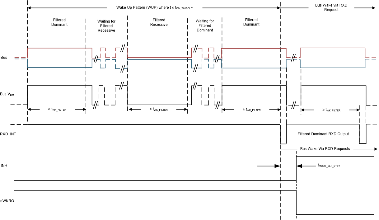
As the TCAN4550 supports low power sleep mode and uses a wake up from the CAN bus mechanism called bus wake via RXD_INT Request (BWRR). Once this pattern is received, the TCAN4550 automatically switches to standby mode and inserts an interrupt onto the nINT and nWKRQ pins to indicate to a host microprocessor that the bus is active, and it should wake up and service the TCAN4550. The low power receiver and bus monitor are enabled in sleep mode to allow for RXD_INT Wake Requests via the CAN bus. A wake up request is output to the internal RXD_INT (driven low) as shown in Figure 25. The wake logic monitors RXD_INT for transitions (high to low) and reactivate the device to standby mode based on the RXD_INT Wake Request. The CAN bus terminals are weakly pulled to GND during this mode, see Figure 4.
These devices use the wake up pattern (WUP) from ISO 11898-2:2016 to qualify bus traffic into a request to wake the host microprocessor. The bus wake request is signaled to the integrated CAN FD controller by a falling edge and low corresponding to a “filtered” bus dominant on the RXD_INT terminal (BWRR).
The wake up pattern (WUP) consists of
- A filtered dominant bus of at least tWK_FILTER followed by
- A filtered recessive bus time of at least tWK_FILTER followed by
- A second filtered dominant bus time of at least tWK_FILTER
Once the WUP is detected, the device starts issuing wake up requests (BWRR) on the RXD_INT signal every time a filtered dominant time is received from the bus. The first filtered dominant initiates the WUP and the bus monitor is now waiting on a filtered recessive, other bus traffic does not reset the bus monitor. Once a filtered recessive is received, the bus monitor is now waiting on a filtered dominant and again, other bus traffic does not reset the bus monitor. Immediately upon receiving of the second filtered dominant the bus monitor recognizes the WUP and transition to BWRR output. Immediately upon verification receiving a WUP the device transitions the bus monitor into BWRR mode, and indicates all filtered dominant bus times on the RXD_INT internal signal by driving it low for the dominant bus time that is in excess of tWK_FILTER, thus the RXD_INT output during BWRR matches the classical 8 pin CAN devices that used the single filtered dominant on the bus as the wake up request mechanism from ISO 11898-2:2016.
For a dominant or recessive to be considered “filtered”, the bus must be in that state for more than tWK_FILTER time. Due to variability in the tWK_FILTER the following scenarios are applicable.
- Bus state times less than tWK_FILTER(MIN) are never detected as part of a WUP, and thus no BWRR is generated.
- Bus state times between tWK_FILTER(MIN) and tWK_FILTER(MAX) may be detected as part of a WUP and a BWRR may be generated.
- Bus state times more than tWK_FILTER(MAX) is always detected as part of a WUP, and thus, a BWRR is always be generated.
See Figure 24 for the timing diagram of the WUP.
The pattern and tWK_FILTER time used for the WUP and BWRR prevents noise and bus stuck dominant faults from causing false wake requests while allowing any CAN or CAN FD message to initiate a BWRR. If the device is switched to normal mode or an under voltage event occurs on VCC the BWRR is lost. The WUP pattern must take place within the tWK_TIMEOUT time otherwise the device is in a state waiting for the next recessive and then a valid WUP pattern.
 Figure 24. Wake Up Pattern (WUP) and Bus Wake via RXD_INT Request (BWRR)
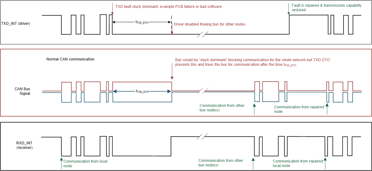
  Figure 25. Example timing diagram with TXD_INT DTO