ZHCSJ48F December 2016 – December 2018 TDA2P-ABZ
ADVANCE INFORMATION for pre-production products; subject to change without notice.
- 1器件概述
- 2修订历史记录
- 3Device Comparison
-
4Terminal Configuration and Functions
- 4.1 Pin Diagram
- 4.2 Pin Attributes
- 4.3 Signal Descriptions
- 4.4 Pin Multiplexing
- 4.5 Connections for Unused Pins
-
5Specifications
- 5.1 Absolute Maximum Ratings
- 5.2 ESD Ratings
- 5.3 Power-On Hours (POH) Limits
- 5.4 Recommended Operating Conditions
- 5.5 Operating Performance Points
- 5.6 Power Consumption Summary
- 5.7
Electrical Characteristics
- Table 5-6 LVCMOS DDR DC Electrical Characteristics
- Table 5-7 Dual Voltage LVCMOS I2C DC Electrical Characteristics
- Table 5-8 IQ1833 Buffers DC Electrical Characteristics
- Table 5-9 IHHV1833 Buffers DC Electrical Characteristics
- Table 5-10 LVCMOS OSC Buffers DC Electrical Characteristics
- Table 5-11 BC1833IHHV Buffers DC Electrical Characteristics
- Table 5-12 Dual Voltage SDIO1833 DC Electrical Characteristics
- Table 5-13 Dual Voltage LVCMOS DC Electrical Characteristics
- 5.7.1 HDMIPHY DC Electrical Characteristics
- 5.7.2 SATAPHY DC Electrical Characteristics
- 5.7.3 USBPHY DC Electrical Characteristics
- 5.7.4 PCIEPHY DC Electrical Characteristics
- 5.8 VPP Specifications for One-Time Programmable (OTP) eFuses
- 5.9 Thermal Resistance Characteristics
- 5.10
Timing Requirements and Switching Characteristics
- 5.10.1 Timing Parameters and Information
- 5.10.2 Interface Clock Specifications
- 5.10.3 Power Supply Sequences
- 5.10.4 Clock Specifications
- 5.10.5 Recommended Clock and Control Signal Transition Behavior
- 5.10.6
Peripherals
- 5.10.6.1 Timing Test Conditions
- 5.10.6.2 Virtual and Manual I/O Timing Modes
- 5.10.6.3 VIP
- 5.10.6.4 DSS
- 5.10.6.5 HDMI
- 5.10.6.6 EMIF
- 5.10.6.7 GPMC
- 5.10.6.8 Timers
- 5.10.6.9 I2C
- 5.10.6.10 UART
- 5.10.6.11 McSPI
- 5.10.6.12 QSPI
- 5.10.6.13
McASP
- Table 5-74 Timing Requirements for McASP1
- Table 5-75 Timing Requirements for McASP2
- Table 5-76 Timing Requirements for McASP3/4/5/6/7/8
- Table 5-77 Switching Characteristics Over Recommended Operating Conditions for McASP1
- Table 5-78 Switching Characteristics Over Recommended Operating Conditions for McASP2
- Table 5-79 Switching Characteristics Over Recommended Operating Conditions for McASP3/4/5/6/7/8
- 5.10.6.14 USB
- 5.10.6.15 SATA
- 5.10.6.16 PCIe
- 5.10.6.17 CAN
- 5.10.6.18
GMAC_SW
- 5.10.6.18.1
GMAC MII Timings
- Table 5-96 Timing Requirements for miin_rxclk - MII Operation
- Table 5-97 Timing Requirements for miin_txclk - MII Operation
- Table 5-98 Timing Requirements for GMAC MIIn Receive 10/100 Mbit/s
- Table 5-99 Switching Characteristics Over Recommended Operating Conditions for GMAC MIIn Transmit 10/100 Mbits/s
- 5.10.6.18.2 GMAC MDIO Interface Timings
- 5.10.6.18.3
GMAC RMII Timings
- Table 5-104 Timing Requirements for GMAC REF_CLK - RMII Operation
- Table 5-105 Timing Requirements for GMAC RMIIn Receive
- Table 5-106 Switching Characteristics Over Recommended Operating Conditions for GMAC REF_CLK - RMII Operation
- Table 5-107 Switching Characteristics Over Recommended Operating Conditions for GMAC RMIIn Transmit 10/100 Mbits/s
- 5.10.6.18.4
GMAC RGMII Timings
- Table 5-111 Timing Requirements for rgmiin_rxc - RGMIIn Operation
- Table 5-112 Timing Requirements for GMAC RGMIIn Input Receive for 10/100/1000 Mbps
- Table 5-113 Switching Characteristics Over Recommended Operating Conditions for rgmiin_txctl - RGMIIn Operation for 10/100/1000 Mbit/s
- Table 5-114 Switching Characteristics for GMAC RGMIIn Output Transmit for 10/100/1000 Mbps
- 5.10.6.18.1
GMAC MII Timings
- 5.10.6.19
eMMC/SD/SDIO
- 5.10.6.19.1
MMC1—SD Card Interface
- 5.10.6.19.1.1 Default speed, 4-bit data, SDR, half-cycle
- 5.10.6.19.1.2 High speed, 4-bit data, SDR, half-cycle
- 5.10.6.19.1.3 SDR12, 4-bit data, half-cycle
- 5.10.6.19.1.4 SDR25, 4-bit data, half-cycle
- 5.10.6.19.1.5 UHS-I SDR50, 4-bit data, half-cycle
- 5.10.6.19.1.6 UHS-I SDR104, 4-bit data, half-cycle
- 5.10.6.19.1.7 UHS-I DDR50, 4-bit data
- 5.10.6.19.2 MMC2 — eMMC
- 5.10.6.19.3 MMC3 and MMC4—SDIO/SD
- 5.10.6.19.1
MMC1—SD Card Interface
- 5.10.6.20 GPIO
- 5.10.6.21 System and Miscellaneous interfaces
- 5.10.7
Emulation and Debug Subsystem
- 5.10.7.1
JTAG
- 5.10.7.1.1
JTAG Electrical Data/Timing
- Table 5-163 Timing Requirements for IEEE 1149.1 JTAG
- Table 5-164 Switching Characteristics Over Recommended Operating Conditions for IEEE 1149.1 JTAG
- Table 5-165 Timing Requirements for IEEE 1149.1 JTAG With RTCK
- Table 5-166 Switching Characteristics Over Recommended Operating Conditions for IEEE 1149.1 JTAG With RTCK
- 5.10.7.1.1
JTAG Electrical Data/Timing
- 5.10.7.2 Trace Port Interface Unit (TPIU)
- 5.10.7.1
JTAG
-
6Detailed Description
- 6.1 Description
- 6.2 Functional Block Diagram
- 6.3 MPU
- 6.4 DSP Subsystem
- 6.5 ISS
- 6.6 IVA
- 6.7 EVE
- 6.8 IPU
- 6.9 VPE
- 6.10 GPU
- 6.11 Memory Subsystem
- 6.12 Interprocessor Communication
- 6.13 Interrupt Controller
- 6.14 EDMA
- 6.15 Peripherals
- 6.16 On-Chip Debug
-
7Applications, Implementation, and Layout
- 7.1 Introduction
- 7.2 Power Optimizations
- 7.3 Core Power Domains
- 7.4 Single-Ended Interfaces
- 7.5
Differential Interfaces
- 7.5.1 General Routing Guidelines
- 7.5.2
USB 2.0 Board Design and Layout Guidelines
- 7.5.2.1 Background
- 7.5.2.2
USB PHY Layout Guide
- 7.5.2.2.1 General Routing and Placement
- 7.5.2.2.2
Specific Guidelines for USB PHY Layout
- 7.5.2.2.2.1 Analog, PLL, and Digital Power Supply Filtering
- 7.5.2.2.2.2 Analog, Digital, and PLL Partitioning
- 7.5.2.2.2.3 Board Stackup
- 7.5.2.2.2.4 Cable Connector Socket
- 7.5.2.2.2.5 Clock Routings
- 7.5.2.2.2.6 Crystals/Oscillator
- 7.5.2.2.2.7 DP/DM Trace
- 7.5.2.2.2.8 DP/DM Vias
- 7.5.2.2.2.9 Image Planes
- 7.5.2.2.2.10 JTAG Interface
- 7.5.2.2.2.11 Power Regulators
- 7.5.2.3 Electrostatic Discharge (ESD)
- 7.5.2.4 References
- 7.5.3 USB 3.0 Board Design and Layout Guidelines
- 7.5.4 HDMI Board Design and Layout Guidelines
- 7.5.5 SATA Board Design and Layout Guidelines
- 7.5.6 PCIe Board Design and Layout Guidelines
- 7.6 Clock Routing Guidelines
- 7.7
DDR2/DDR3 Board Design and Layout Guidelines
- 7.7.1 DDR2/DDR3 General Board Layout Guidelines
- 7.7.2 DDR2 Board Design and Layout Guidelines
- 7.7.3
DDR3 Board Design and Layout Guidelines
- 7.7.3.1 Board Designs
- 7.7.3.2 DDR3 EMIF
- 7.7.3.3 DDR3 Device Combinations
- 7.7.3.4 DDR3 Interface Schematic
- 7.7.3.5 Compatible JEDEC DDR3 Devices
- 7.7.3.6 PCB Stackup
- 7.7.3.7 Placement
- 7.7.3.8 DDR3 Keepout Region
- 7.7.3.9 Bulk Bypass Capacitors
- 7.7.3.10 High-Speed Bypass Capacitors
- 7.7.3.11 Net Classes
- 7.7.3.12 DDR3 Signal Termination
- 7.7.3.13 VREF_DDR Routing
- 7.7.3.14 VTT
- 7.7.3.15 CK and ADDR_CTRL Topologies and Routing Definition
- 7.7.3.16 Data Topologies and Routing Definition
- 7.7.3.17 Routing Specification
- 8Device and Documentation Support
- 9Mechanical Packaging Information
7.2.3 Step 3: Static Analysis
Delivering reliable power to circuits is always of critical importance because voltage drops (also known as IR drops) can happen at every level within an electronic system, on-chip, within a package, and across the board. Robust system performance can only be ensured by understanding how the system elements will perform under typical stressful Use Cases. Therefore, it is a good practice to perform a Static or DC Analysis.
Static or DC analysis and design methodology results in a PDN design that minimizes voltage or IR drops across power and ground planes, traces and vias. This ensures the application processor’s internal transistors will be operating within their specified voltage ranges for proper functionality. The amount of IR drop that will be encounter is based upon amount power drawn for a desired Use Case and PCB trace (widths, geometry and number of parallel traces) and via (size, type and number) characteristics.
Components that are distant from their power source are particularly susceptible to IR drop. Designs that rely on battery power must minimize voltage drops to avoid unacceptable power loss that can negatively impact system performance. Early assessments a PDN’s static (DC) performance helps to determine basic power distribution parameters such as best system input power point, optimal PCB layer stackup, and copper area needed for load currents.
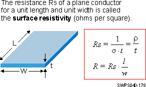
 Figure 7-9 Depiction of Sheet Resistivity and Resistance
 Ohm’s Law (V = I × R) relates conduction current to voltage drop. At DC, the relation coefficient is a constant and represents the resistance of the conductor. Even current carrying conductors will dissipate power at high currents even though their resistance may be very small. Both voltage drop and power dissipation are proportional to the resistance of the conductor.
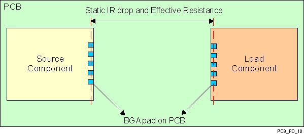
Figure 7-10 shows a PCB-level static IR drop budget defined between the power management device (PMIC) pins and the application processor’s balls when the PMIC is supplying power.
- It is highly recommended to physically place the PMIC as close as possible to the processor and on the same side. The orientation of the PMIC vs. processor should be aligned to minimize distance for the highest current rail.
 Figure 7-10 Static IR Drop Budget for PCB Only
 The system-level IR drop budget is made up of three portions: on-chip, package, and PCB board. Static IR or DC analysis/design methodology consists of designing the PDN such that the voltage drop (under DC operating conditions) across power and ground pads of the transistors of the application processor device is within a specified value of the nominal voltage for proper functionality of the device.
A PCB system-level voltage drop budget for proper device functionality is typically 1.5 % of nominal voltage. For a 1.35-V supply, this would be ≤ 20 mV.
To accurately analyze PCB static IR drop, the actual geometry of the PDN must be modeled properly and simulated to accurately characterize long distribution paths, copper weight impacts, electro-migration violations of current-carrying vias, and “Swiss-cheese” effects via placement has on power rails. It is recommended to perform the following analyses:
- Lumped resistance/IR drop analysis
- Distributed resistance/IR drop analysis
NOTE
The PMIC companion device supporting Processor has been designed with voltage sensing feedback loop capabilities that enable a remote sense of the SMPS output voltage at the point of use.
The NOTE above means the SMPS feedback signals and returns must be routed across PCB and connected to the Device input power ball for which a particular SMPS is supplying power. This feedback loop provides compensation for some of the voltage drop encountered across the PDN within limits. As such, the effective resistance of the PDN within this loop should be determined in order to optimize voltage compensation loop performance. The resistance of two PDN segments are of interest: one from the power inductor/bulk power filtering capacitor node to the Processor’s input power and second is the entire PDN route from SMPS output pin/ball to the Processor input power.
In the following sections each methodology is described in detail and an example has been provided of analysis flow that can be used by the PCB designer to validate compliance to the requirements on their PCB PDN design.