ZHCSJ48F December 2016 – December 2018 TDA2P-ABZ
ADVANCE INFORMATION for pre-production products; subject to change without notice.
- 1器件概述
- 2修订历史记录
- 3Device Comparison
-
4Terminal Configuration and Functions
- 4.1 Pin Diagram
- 4.2 Pin Attributes
- 4.3 Signal Descriptions
- 4.4 Pin Multiplexing
- 4.5 Connections for Unused Pins
-
5Specifications
- 5.1 Absolute Maximum Ratings
- 5.2 ESD Ratings
- 5.3 Power-On Hours (POH) Limits
- 5.4 Recommended Operating Conditions
- 5.5 Operating Performance Points
- 5.6 Power Consumption Summary
- 5.7
Electrical Characteristics
- Table 5-6 LVCMOS DDR DC Electrical Characteristics
- Table 5-7 Dual Voltage LVCMOS I2C DC Electrical Characteristics
- Table 5-8 IQ1833 Buffers DC Electrical Characteristics
- Table 5-9 IHHV1833 Buffers DC Electrical Characteristics
- Table 5-10 LVCMOS OSC Buffers DC Electrical Characteristics
- Table 5-11 BC1833IHHV Buffers DC Electrical Characteristics
- Table 5-12 Dual Voltage SDIO1833 DC Electrical Characteristics
- Table 5-13 Dual Voltage LVCMOS DC Electrical Characteristics
- 5.7.1 HDMIPHY DC Electrical Characteristics
- 5.7.2 SATAPHY DC Electrical Characteristics
- 5.7.3 USBPHY DC Electrical Characteristics
- 5.7.4 PCIEPHY DC Electrical Characteristics
- 5.8 VPP Specifications for One-Time Programmable (OTP) eFuses
- 5.9 Thermal Resistance Characteristics
- 5.10
Timing Requirements and Switching Characteristics
- 5.10.1 Timing Parameters and Information
- 5.10.2 Interface Clock Specifications
- 5.10.3 Power Supply Sequences
- 5.10.4 Clock Specifications
- 5.10.5 Recommended Clock and Control Signal Transition Behavior
- 5.10.6
Peripherals
- 5.10.6.1 Timing Test Conditions
- 5.10.6.2 Virtual and Manual I/O Timing Modes
- 5.10.6.3 VIP
- 5.10.6.4 DSS
- 5.10.6.5 HDMI
- 5.10.6.6 EMIF
- 5.10.6.7 GPMC
- 5.10.6.8 Timers
- 5.10.6.9 I2C
- 5.10.6.10 UART
- 5.10.6.11 McSPI
- 5.10.6.12 QSPI
- 5.10.6.13
McASP
- Table 5-74 Timing Requirements for McASP1
- Table 5-75 Timing Requirements for McASP2
- Table 5-76 Timing Requirements for McASP3/4/5/6/7/8
- Table 5-77 Switching Characteristics Over Recommended Operating Conditions for McASP1
- Table 5-78 Switching Characteristics Over Recommended Operating Conditions for McASP2
- Table 5-79 Switching Characteristics Over Recommended Operating Conditions for McASP3/4/5/6/7/8
- 5.10.6.14 USB
- 5.10.6.15 SATA
- 5.10.6.16 PCIe
- 5.10.6.17 CAN
- 5.10.6.18
GMAC_SW
- 5.10.6.18.1
GMAC MII Timings
- Table 5-96 Timing Requirements for miin_rxclk - MII Operation
- Table 5-97 Timing Requirements for miin_txclk - MII Operation
- Table 5-98 Timing Requirements for GMAC MIIn Receive 10/100 Mbit/s
- Table 5-99 Switching Characteristics Over Recommended Operating Conditions for GMAC MIIn Transmit 10/100 Mbits/s
- 5.10.6.18.2 GMAC MDIO Interface Timings
- 5.10.6.18.3
GMAC RMII Timings
- Table 5-104 Timing Requirements for GMAC REF_CLK - RMII Operation
- Table 5-105 Timing Requirements for GMAC RMIIn Receive
- Table 5-106 Switching Characteristics Over Recommended Operating Conditions for GMAC REF_CLK - RMII Operation
- Table 5-107 Switching Characteristics Over Recommended Operating Conditions for GMAC RMIIn Transmit 10/100 Mbits/s
- 5.10.6.18.4
GMAC RGMII Timings
- Table 5-111 Timing Requirements for rgmiin_rxc - RGMIIn Operation
- Table 5-112 Timing Requirements for GMAC RGMIIn Input Receive for 10/100/1000 Mbps
- Table 5-113 Switching Characteristics Over Recommended Operating Conditions for rgmiin_txctl - RGMIIn Operation for 10/100/1000 Mbit/s
- Table 5-114 Switching Characteristics for GMAC RGMIIn Output Transmit for 10/100/1000 Mbps
- 5.10.6.18.1
GMAC MII Timings
- 5.10.6.19
eMMC/SD/SDIO
- 5.10.6.19.1
MMC1—SD Card Interface
- 5.10.6.19.1.1 Default speed, 4-bit data, SDR, half-cycle
- 5.10.6.19.1.2 High speed, 4-bit data, SDR, half-cycle
- 5.10.6.19.1.3 SDR12, 4-bit data, half-cycle
- 5.10.6.19.1.4 SDR25, 4-bit data, half-cycle
- 5.10.6.19.1.5 UHS-I SDR50, 4-bit data, half-cycle
- 5.10.6.19.1.6 UHS-I SDR104, 4-bit data, half-cycle
- 5.10.6.19.1.7 UHS-I DDR50, 4-bit data
- 5.10.6.19.2 MMC2 — eMMC
- 5.10.6.19.3 MMC3 and MMC4—SDIO/SD
- 5.10.6.19.1
MMC1—SD Card Interface
- 5.10.6.20 GPIO
- 5.10.6.21 System and Miscellaneous interfaces
- 5.10.7
Emulation and Debug Subsystem
- 5.10.7.1
JTAG
- 5.10.7.1.1
JTAG Electrical Data/Timing
- Table 5-163 Timing Requirements for IEEE 1149.1 JTAG
- Table 5-164 Switching Characteristics Over Recommended Operating Conditions for IEEE 1149.1 JTAG
- Table 5-165 Timing Requirements for IEEE 1149.1 JTAG With RTCK
- Table 5-166 Switching Characteristics Over Recommended Operating Conditions for IEEE 1149.1 JTAG With RTCK
- 5.10.7.1.1
JTAG Electrical Data/Timing
- 5.10.7.2 Trace Port Interface Unit (TPIU)
- 5.10.7.1
JTAG
-
6Detailed Description
- 6.1 Description
- 6.2 Functional Block Diagram
- 6.3 MPU
- 6.4 DSP Subsystem
- 6.5 ISS
- 6.6 IVA
- 6.7 EVE
- 6.8 IPU
- 6.9 VPE
- 6.10 GPU
- 6.11 Memory Subsystem
- 6.12 Interprocessor Communication
- 6.13 Interrupt Controller
- 6.14 EDMA
- 6.15 Peripherals
- 6.16 On-Chip Debug
-
7Applications, Implementation, and Layout
- 7.1 Introduction
- 7.2 Power Optimizations
- 7.3 Core Power Domains
- 7.4 Single-Ended Interfaces
- 7.5
Differential Interfaces
- 7.5.1 General Routing Guidelines
- 7.5.2
USB 2.0 Board Design and Layout Guidelines
- 7.5.2.1 Background
- 7.5.2.2
USB PHY Layout Guide
- 7.5.2.2.1 General Routing and Placement
- 7.5.2.2.2
Specific Guidelines for USB PHY Layout
- 7.5.2.2.2.1 Analog, PLL, and Digital Power Supply Filtering
- 7.5.2.2.2.2 Analog, Digital, and PLL Partitioning
- 7.5.2.2.2.3 Board Stackup
- 7.5.2.2.2.4 Cable Connector Socket
- 7.5.2.2.2.5 Clock Routings
- 7.5.2.2.2.6 Crystals/Oscillator
- 7.5.2.2.2.7 DP/DM Trace
- 7.5.2.2.2.8 DP/DM Vias
- 7.5.2.2.2.9 Image Planes
- 7.5.2.2.2.10 JTAG Interface
- 7.5.2.2.2.11 Power Regulators
- 7.5.2.3 Electrostatic Discharge (ESD)
- 7.5.2.4 References
- 7.5.3 USB 3.0 Board Design and Layout Guidelines
- 7.5.4 HDMI Board Design and Layout Guidelines
- 7.5.5 SATA Board Design and Layout Guidelines
- 7.5.6 PCIe Board Design and Layout Guidelines
- 7.6 Clock Routing Guidelines
- 7.7
DDR2/DDR3 Board Design and Layout Guidelines
- 7.7.1 DDR2/DDR3 General Board Layout Guidelines
- 7.7.2 DDR2 Board Design and Layout Guidelines
- 7.7.3
DDR3 Board Design and Layout Guidelines
- 7.7.3.1 Board Designs
- 7.7.3.2 DDR3 EMIF
- 7.7.3.3 DDR3 Device Combinations
- 7.7.3.4 DDR3 Interface Schematic
- 7.7.3.5 Compatible JEDEC DDR3 Devices
- 7.7.3.6 PCB Stackup
- 7.7.3.7 Placement
- 7.7.3.8 DDR3 Keepout Region
- 7.7.3.9 Bulk Bypass Capacitors
- 7.7.3.10 High-Speed Bypass Capacitors
- 7.7.3.11 Net Classes
- 7.7.3.12 DDR3 Signal Termination
- 7.7.3.13 VREF_DDR Routing
- 7.7.3.14 VTT
- 7.7.3.15 CK and ADDR_CTRL Topologies and Routing Definition
- 7.7.3.16 Data Topologies and Routing Definition
- 7.7.3.17 Routing Specification
- 8Device and Documentation Support
- 9Mechanical Packaging Information
5.10.3 Power Supply Sequences
This section describes the power-up and power-down sequence required to ensure proper device operation. The power supply names described in this section comprise a superset of a family of compatible devices. Some members of this family will not include a subset of these power supplies and their associated device modules. Refer to Section 4.2, Pin Attributes for a specific device to determine which power supplies are applicable.
NOTE
For more information, see Power, Reset and Clock Management / Reset Management Functional Description / Reset Sequences of the Device TRM.
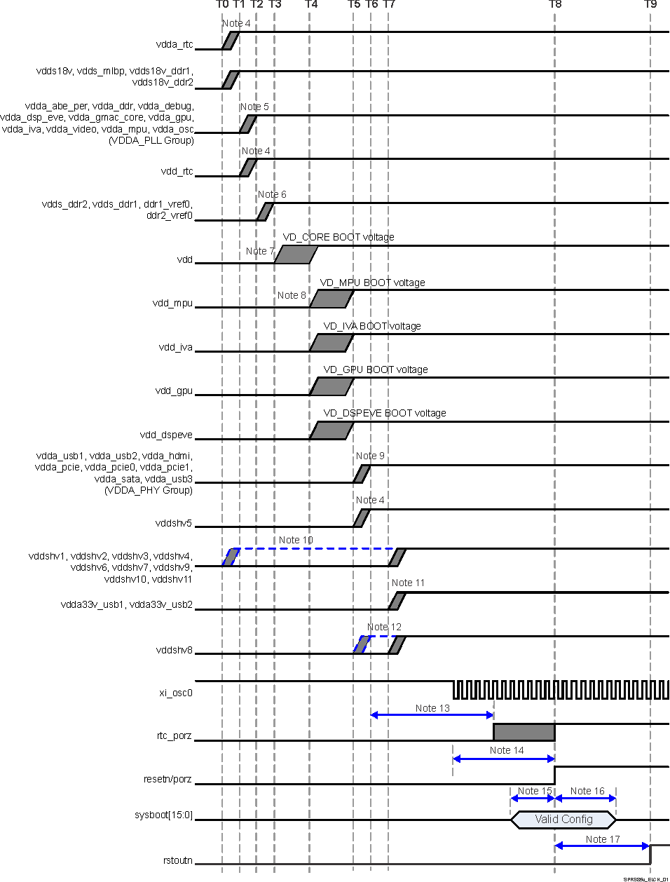
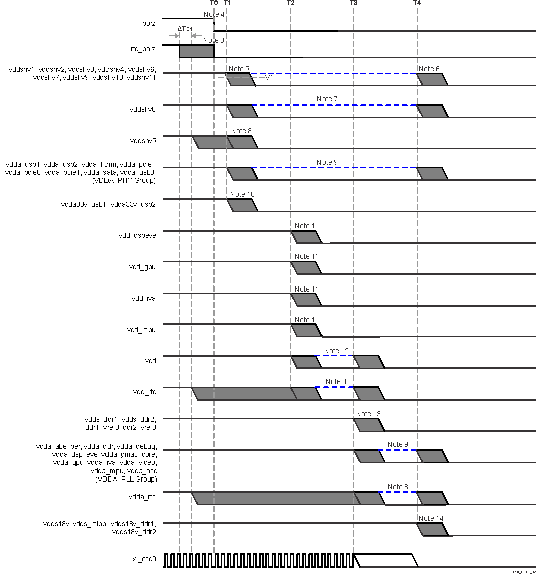
Figure 5-5 and Figure 5-6, describes the device power sequencing.
 Figure 5-5 Recommended Power-Up Sequencing
 - Time stamps:
- T0 = 0 ms; T1 = 0.55 ms; T2 = 1.1 ms; T3 = 1.65 ms; T4 = 2.2 ms; T5 = 2.75 ms; T6 = 3.3 ms; T7 = 5.85 ms; T8 = 6.4 ms; T9 = 8.4 ms. All “Tn” markers show total elapsed time from T0.
- Terminology:
- VOPR MIN = Minimum Operational Voltage level that ensures device functionality and specified performance per Section 5.4, Recommended Operating Conditions.
- Ramp Up = transition time from VOFF to VOPR MIN.
- General timing diagram items:
- Grey shaded areas show valid transition times for supplies between VOPR MIN and VOFF.
- Dashed horizontal lines are not valid ramp times but show alternate transition times based upon common sources and clarified in associated note.
- Dashed vertical lines show approximate elapse times based upon TI recommended PMIC power sequencer circuit performance.
- vddshv5, vdd_rtc, and vdda_rtc domains:
- If RTC mode is used, then vdda_rtc, vdd_rtc and vddshv5 must be individually powered with separate power supplies and cannot be combined with other rails.
- If RTC-mode is not supported then the following combinations are approved:
- vdda_rtc can be combined with vdds18v
- vdd_rtc can be combined with vdd
- vddshv5 can be combined with other 1.8 V or 3.3 V vddshvn rails
- vdda_* rails should not be combined with vdds18v_* for best performance to avoid transient switching noise impacts on analog domains. vdda_* should not ramp-up before vdds18v_* but could ramp concurrently if design ensures final operational voltage will not be reached until after vdds18v. The preferred sequence is to follow all vdds18v_* to ensure circuit components and PCB design do not cause an inadvertent violation.
- vdds_ddr* should not ramp-up before vdds18v_*. The preferred sequence has vdds_ddr1 following vdds18v_* to ensure circuit components and PCB design do not cause an inadvertent violation. vdds_ddr1 can ramp-up before, concurrently or after vdda_*, there are no dependencies between vdds_ddr1 and vdda_* domains.
- vdd should not ramp-up before vdds18v_* or vdds_ddr* domains have reached VOPR MIN.
- vdd_mpu, vdd_iva, vdd_gpu, vdd_dspeve domains should follow vdd core supply as preferred sequence. If vdd_mpu, vdd_iva, vdd_gpu, vdd_dspeve domains ramp concurrently or quicker than vdd core, then vdd core must remain at least 150 mV greater than vdd_mpu, vdd_iva, vdd_gpu, vdd_dspeve domains during ramp. Circuit design (components and PCB) must ensure vdd reaches final operational voltage before any of the vdd_mpu, vdd_iva, vdd_gpu, vdd_dspeve domains.
- VDDA_PHY group should not be combined with VDDA_PLL group to avoid transient switching noise impacts.
- vddshv[1-4, 6, 7, 9-11] domains:
- If 1.8 V I/O signaling is needed, then 1.8 V must be sourced from common vdds18v supply and ramp up concurrently with vdds18v.
- If 3.3 V I/O signaling is needed, then 3.3 V vddshvx rails must ramp up after vdd_mpu, vdd_iva, vdd_gpu, vdd_dspeve, and VDDA_PHY group domains.
- vdda33v_usb[1-2] domain:
- If USB1 and USB2 interfaces are used, should be supplied from independent analog supply.
- If USB1/USB2 interface is not used, could be connected to VSS/GND if both conditions are met:
- USB1/USB2 diff pair (usb1_dm/usb1_dp; usb2_dm/usb2_dp) pins are left unconnected
- vdda_usb1 and/or vdda_usb2 PHY is not energized
- vddshv8 shows two ramp up options for 1.8 V I/O or 3.3 V I/O or SD Card operation:
- If 1.8 V I/O signaling is needed, then vddshv8 must ramp up after vdd and before or concurrently with 3.3 V vddshv* rails.
- If 3.3 V I/O signaling is needed, then vddshv8 must be combined with other 3.3 V vddshv* rails.
- If SD Card operation is needed, then vddshv8 must be sourced from a dual voltage (3.3 V / 1.8 V) power source per SDIO specifications and ramp up concurrently with 3.3 V vddshv* rails.
- Pulse duration: rtc_porz must remain low 1ms after vdda_rtc, vddshv5, and vdd_rtc are ramped and stable or can be de-asserted before but no later than porz. The FUNK_32K_CLK source must be stable and at a valid frequency 1 ms prior to de-asserting rtc_porz high.
- porz must remain asserted low until both of the following conditions are met:
- Minimum of 12 × P, where P = 1 / (SYS_CLK1 / 610), units in ns.
- All device supply rails reach stable operational levels.
- Setup time: sysboot[15:0] pins must be valid 2P(14) before porz is de-asserted high.
- Hold time: sysboot[15:0] pins must be valid 15P(14) after porz is de-asserted high.
- rstoutn will be set high after global reset, due to porz, is de-asserted following an internal 2 ms delay. rstoutn is only valid after vddshv3 reaches an operational level. If used as a peripheral component reset, it should be AND gated with porz to avoid possible reset glitches during power up.
 Figure 5-6 Recommended Power-Down Sequencing
 - Time stamps:
- T0 = 0 ms, T1 > 100 μs, T2 = 0.5 ms, T3 = 1.0 ms, T4 = 1.5 ms; V1 = 2.7 V. All “Tn” markers are intended to show elapsed times from T0. Delta time: Δ TD1 > 100 μs.
- Terminology:
- VOPR MIN = Minimum Operational Voltage level that ensures device functionality and specified performance per Section 5.4, Recommended Operating Conditions.
- VOFF = OFF Voltage level is defined to be less than 0.6 V where any current draw has no impact to POH.
- Ramp Down = transition time from VOPR MIN to VOFF and is slew rate independent.
- General timing diagram items:
- Grey shaded areas show valid transition times for supplies between VOPR MIN and VOFF.
- Dashed horizontal lines are not valid ramp times but show alternate transition times based upon common sources and clarified in associated note.
- Dashed vertical lines show approximate elapse times based upon TI recommended PMIC power-down sequencer circuit performance.
- porz signals must be asserted low for 100 µs min to ensure SoC is set to a safe functional state before any voltage begins to ramp down.
- vddshv* domains supplied by 3.3 V:
- must remain greater than 2.7 V to enable Dual Voltage GPIO selector circuit operation for 100 µs min after porz is asserted low.
- must be in first group of supplies ramping down after porz has been asserted low for 100 µs min.
- must not exceed vdds18v by more than 2 V during ramp down, see Figure 5-10 “vdds18v and vdda_* Discharge Relationship”.
- vddshv* domains supplied by 1.8 V:
- must ramp down concurrently with vdds18v and be sourced from the same vdds18v supply.
- vddshv8 domain:
- must be in first group of supplies to ramp down after porz has been asserted low for 100 µs min.
- if SDIO operation is needed, must be sourced from independent power resource that can provide dual voltage (3.3 V / 1.8 V) operation as required to be compliant to SDIO specification
- if SDIO operation is not needed, must be grouped and ramped down with other vddshv* domains as noted above.
- RTC domains (vddshv5, vdd_rtc, and vdda_rtc):
- If RTC mode is used:
- rtc_porz can be asserted low before porz and RTC domains can be ramped down after 100 µs elapsed time.
- must be sourced from independent supplies and must not be combined with other rails.
- timing diagram shows this mode of operation.
- If RTC mode is not used, then:
- rtc_porz must be connected to porz signal.
- vddshv5 must be grouped and ramped down with other vddshv* domains as noted above.
- vdd_rtc must be grouped and ramped down with vdd.
- vdda_rtc must be grouped and ramped down with either VDDA_PHY group or vdds18v.
- If RTC mode is used:
- vdda_* domains:
- should not be combined with vdds18v for best performance to avoid transient switching noise impacts on analog domains.
- can ramp down before or concurrently with vdds18v.
- must satisfy the vdds18v and vdda_* Discharge Relationship (see Figure 5-10) if vdda_* disable point is later or discharge rate is slower than vdds18v.
- can ramp down before, concurrently or after vdds_ddr*, there is no dependency between these supplies.
- vdda33v_usb* domains:
- can start ramping down 100 µs after low assertion of porz
- can ramp down concurrently or before VDDA_PHY group
- vdd_dspeve, vdd_gpu, vdd_iva, vdd_mpu domains can ramp down before or concurrently with vdd.
- vdd can ramp down concurrently or after with vdd_dspeve, vdd_gpu, vdd_iva, vdd_mpu domains.
- vdds_ddr* domains:
- should ramp down after vdd begins ramping down.
- vdds18v domain:
- should maintain VOPR MIN (VNOM -5% = 1.71 V) until all other supplies start to ramp down.
- must satisfy the vdds18v versus vddshv[1-7, 9-11] Discharge Relationship (see Figure 5-8) if vddshv* is operating at 3.3 V
- must satisfy the vdds18v and vdds_ddr* Discharge Relationship (see Figure 5-9) if vdds_ddr* discharge rate is slower than vdds18v.
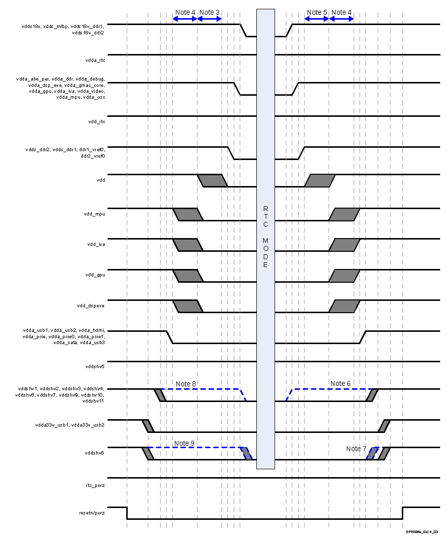
Figure 5-7 describes the RTC-mode power sequencing.
 Figure 5-7 RTC Mode Sequencing
 - Grey shaded areas are windows where it is valid to ramp the voltage rail.
- Blue dashed lines are not valid windows but show alternate ramp possibilities based on the associated note.
- vdd must ramp down after or at the same time as vdd_mpu, vdd_gpu, vdd_dspeve and vdd_iva.
- vdd_mpu, vdd_gpu, vdd_dspeve, vdd_iva can be ramped at the same time or can be staggered.
- vdd must ramp up before or at the same time as vdd_mpu, vdd_gpu, vdd_dspeve and vdd_iva.
- If any of the vddshv[1-7,9-11] rails (not including vddshv8) are used as 1.8 V only, then these rails can be combined with vdds18v.
- vddshv8 is separated out to show support for dual voltage. If single voltage is used then vddshv8 can be combined with other vddshvn rails but vddshv8 must ramp down before vdd and must ramp up after vdd.
- If any of the vddshv[1-7,9-11] rails (not including vddshv8) are used as 1.8 V only, then these rails can be combined with vdds18v. vddshv[1-7,9-11] is allowed to ramp down at either of the two points shown in the timing diagram in either 1.8 V mode or in 3.3 V mode. If vddshv[1-7,9-11] ramps down at the later time in the diagram then the board design must guarantee that the vddshvn rail is never higher than 2.0 V above the vdds18v rail.
- vddshv8 is separated out to show support for dual voltage. If a dedicated LDO/supply source is used for vddshv8, then vddshv8 ramp down should occur at one of the two earliest points in the timing diagram. If vddshv8 is powered by the same supply source as the other vddshvn rails, then it is allowed to ramp down at either of the last two points in the timing diagram.
Figure 5-8 describes vddshv[1-7,9-11] supplies falling before vdds18v supplies delta.
![TDA2P-ABZ vdds18v versus vddshv[1-7, 9-11] Discharge Relationship TDA2P-ABZ SPRS85v_ELCH_06.gif](/ods/images/ZHCSJ48F/SPRS85v_ELCH_06.gif) Figure 5-8 vdds18v versus vddshv[1-7, 9-11] Discharge Relationship
Figure 5-8 vdds18v versus vddshv[1-7, 9-11] Discharge Relationship - Vdelta MAX = 2 V.
- If vddshv8 is powered by the same supply source as the other vddshv[1-7,9-11] rails.
If vdds18v and vdds_ddr* are disabled at the same time due to a loss of input power event or if vdds_ddr* discharges more slowly than vdds18v, analysis has shown no reliability impacts when the elapsed time period beginning with vdds18v dropping below 1.0 V and ending with vdds_ddr* dropping below 0.6 V is less than 10 ms (Figure 5-9).
 Figure 5-9 vdds18v and vdds_ddr* Discharge Relationship(1)
 - V1 > 1.0 V; V2 < 0.6V; T1 < 10ms.
 Figure 5-10 vdds18v and vdda_* Discharge Relationship(3)
 - vdda_* can be ≥ vdds18v, until vdds18v drops below 1.62 V.
- vdds18v must be ≥ vdda_*, until vdds18v reaches 0.6 V.
- V1 = 1.62 V; V2 < 0.6 V.
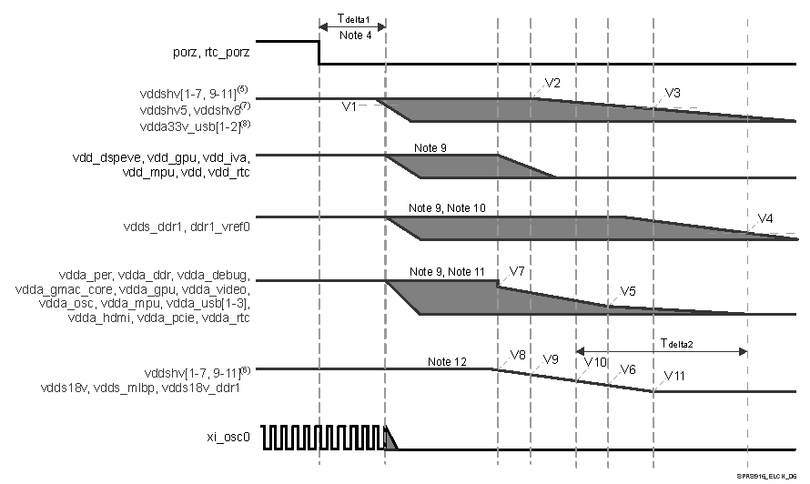
Figure 5-8 through Figure 5-11 and associated notes described the device abrupt power down sequence.
A ”loss of input power event” occurs when the system’s input power is unexpectedly removed. Normally, the recommended power-down sequence should be followed and can be accomplished within 1.5-2 ms of elapsed time. This is the typical range of elapsed time available following a loss of power event, see Section 7.3.7 for design recommendations. If sufficient elapse time is not provided, then an “abrupt” power down sequence can be supported without impacting POH reliability if all of the following conditions are met (Figure 5-11).
 Figure 5-11 Abrupt Power-Down Sequencing(1)
 - Time stamps:
- V1 = 2.7 V; V2 = 3.3 V; V3 = 2.0 V; V4 = V5 = V6 = 0.6 V; V7 = V8 = 1.62 V; V9 = 1.3 V; V10 = 1.0 V; V11 = 0.0 V; Tdelta1 > 100 µs; Tdelta2 < 10 ms.
- Terminology:
- VOPR MIN = Minimum Operational Voltage level that ensures device functionality and specified performance in Section 5.4, Recommended Operating Conditions table.
- VOFF = OFF Voltage level is defined to be less than 0.6 V, where any current draw has no impact to POH.
- Ramp Down = transition time from VOPR MIN to VOFF and is slew rate independent.
- General timing diagram items:
- Grey shaded areas show valid transition times for supplies between VOPR MIN and VOFF.
- Dashed vertical lines show approximate elapse times based upon TI recommended PMIC power-down sequencer circuit performance.
- porz and rtc_porz must be asserted low for 100 μs min to ensure SoC is set to a safe functional state before any voltage begins to ramp down.
- Only if using RTC-mode with an independent RTC input power source, then rtc_porz can remain high and RTC-domains (vdd_rtc, vdda_rtc, and vddshv5) can remain energized while all other domains sourced from the system input power are powered down.
- vddshv[1-7, 9-11] domains supplied by 3.3 V:
- must remain greater than 2.7 V to enable Dual Voltage GPIO selector circuit operation for 100 μs min, after porz is asserted low.
- must not exceed vdds18v voltage level by more than 2 V during ramp down, until vdds18v drops below VOFF (0.6 V).
- vddshv[1-7, 9-11] domains supplied by 1.8 V must ramp down concurrently with vdds18v and be sourced from common vdds18v supply.
- vddshv8 supporting SD Card:
- must be in first group of supplies to ramp down after porz has been asserted low for 100 µs min.
- must be sourced from independent power resource that can provide dual voltage (3.3 V / 1.8 V) operation as required to be compliant to SDIO specification.
- if SDIO operation is not needed, must be grouped with other vddshv[1-7, 9-11] domains.
- vdda33v_usb[1-2] domains must be in first group of supplies to ramp down after porz has been asserted low for 100 µs min.
- vdd_dspeve, vdd_gpu, vdd_iva, vdd_mpu, vdd, vdd_rtc, vdds_ddr1, vdda_* domains can all start to ramp down in any order after 100 µs low assertion of porz.
- vdds_ddr1 domains:
- can remain at VOPR MIN or a level greater than vdds18v during ramp down.
- elapsed time from vdds18v dropping below 1.0 V to vdds_ddr[1-3] dropping below 0.6 V must not exceed 10 ms.
- vdda_* domains:
- can start to ramp down before or concurrently with vdds18v.
- must not exceed vdds18v voltage level after vdds18v drops below 1.62 V until vdds18v drops below VOFF (0.6 V).
- vdds18v domain should maintain a minimum level of 1.62 V (VNOM – 10%) until vdd_dspeve and vdd start to ramp down.