ZHCSJ49F March 2017 – February 2019 TDA2P-ACD
PRODUCTION DATA.
- 1器件概述
- 2修订历史记录
- 3Device Comparison
-
4Terminal Configuration and Functions
- 4.1 Pin Diagram
- 4.2 Pin Attributes
- 4.3
Signal Descriptions
- 4.3.1 VIP
- 4.3.2 DSS
- 4.3.3 HDMI
- 4.3.4 Camera Serial Interface 2 CAL bridge (CSI2)
- 4.3.5 EMIF
- 4.3.6 GPMC
- 4.3.7 Timers
- 4.3.8 I2C
- 4.3.9 UART
- 4.3.10 McSPI
- 4.3.11 QSPI
- 4.3.12 McASP
- 4.3.13 USB
- 4.3.14 SATA
- 4.3.15 PCIe
- 4.3.16 DCAN and MCAN
- 4.3.17 GMAC_SW
- 4.3.18 eMMC/SD/SDIO
- 4.3.19 GPIO
- 4.3.20 PWM
- 4.3.21 System and Miscellaneous
- 4.3.22 Test Interfaces
- 4.4 Pin Multiplexing
- 4.5 Connections for Unused Pins
-
5Specifications
- 5.1 Absolute Maximum Ratings
- 5.2 ESD Ratings
- 5.3 Power-On Hours (POH) Limits
- 5.4 Recommended Operating Conditions
- 5.5 Operating Performance Points
- 5.6 Power Consumption Summary
- 5.7
Electrical Characteristics
- Table 5-6 LVCMOS DDR DC Electrical Characteristics
- Table 5-7 Dual Voltage LVCMOS I2C DC Electrical Characteristics
- Table 5-8 IQ1833 Buffers DC Electrical Characteristics
- Table 5-9 LVCMOS CSI2 DC Electrical Characteristics
- Table 5-10 IHHV1833 Buffers DC Electrical Characteristics
- Table 5-11 Dual Voltage SDIO1833 DC Electrical Characteristics
- Table 5-12 Dual Voltage LVCMOS DC Electrical Characteristics
- 5.7.1 HDMIPHY DC Electrical Characteristics
- 5.7.2 SATAPHY DC Electrical Characteristics
- 5.7.3 USBPHY DC Electrical Characteristics
- 5.7.4 PCIEPHY DC Electrical Characteristics
- 5.8 VPP Specifications for One-Time Programmable (OTP) eFuses
- 5.9 Thermal Resistance Characteristics
- 5.10
Timing Requirements and Switching Characteristics
- 5.10.1 Timing Parameters and Information
- 5.10.2 Interface Clock Specifications
- 5.10.3 Power Supply Sequences
- 5.10.4 Clock Specifications
- 5.10.5 Recommended Clock and Control Signal Transition Behavior
- 5.10.6
Peripherals
- 5.10.6.1 Timing Test Conditions
- 5.10.6.2 Virtual and Manual I/O Timing Modes
- 5.10.6.3 VIP
- 5.10.6.4 DSS
- 5.10.6.5 HDMI
- 5.10.6.6 EMIF
- 5.10.6.7 GPMC
- 5.10.6.8 Timers
- 5.10.6.9 I2C
- 5.10.6.10 UART
- 5.10.6.11 McSPI
- 5.10.6.12 QSPI
- 5.10.6.13
McASP
- Table 5-70 Timing Requirements for McASP1
- Table 5-71 Timing Requirements for McASP2
- Table 5-72 Timing Requirements for McASP3/4/5/6/7/8
- Table 5-73 Switching Characteristics Over Recommended Operating Conditions for McASP1
- Table 5-74 Switching Characteristics Over Recommended Operating Conditions for McASP2
- Table 5-75 Switching Characteristics Over Recommended Operating Conditions for McASP3/4/5/6/7/8
- 5.10.6.14 USB
- 5.10.6.15 SATA
- 5.10.6.16 PCIe
- 5.10.6.17 CAN
- 5.10.6.18
GMAC_SW
- 5.10.6.18.1
GMAC MII Timings
- Table 5-92 Timing Requirements for miin_rxclk - MII Operation
- Table 5-93 Timing Requirements for miin_txclk - MII Operation
- Table 5-94 Timing Requirements for GMAC MIIn Receive 10/100 Mbit/s
- Table 5-95 Switching Characteristics Over Recommended Operating Conditions for GMAC MIIn Transmit 10/100 Mbits/s
- 5.10.6.18.2 GMAC MDIO Interface Timings
- 5.10.6.18.3
GMAC RMII Timings
- Table 5-100 Timing Requirements for GMAC REF_CLK - RMII Operation
- Table 5-101 Timing Requirements for GMAC RMIIn Receive
- Table 5-102 Switching Characteristics Over Recommended Operating Conditions for GMAC REF_CLK - RMII Operation
- Table 5-103 Switching Characteristics Over Recommended Operating Conditions for GMAC RMIIn Transmit 10/100 Mbits/s
- 5.10.6.18.4
GMAC RGMII Timings
- Table 5-107 Timing Requirements for rgmiin_rxc - RGMIIn Operation
- Table 5-108 Timing Requirements for GMAC RGMIIn Input Receive for 10/100/1000 Mbps
- Table 5-109 Switching Characteristics Over Recommended Operating Conditions for rgmiin_txctl - RGMIIn Operation for 10/100/1000 Mbit/s
- Table 5-110 Switching Characteristics for GMAC RGMIIn Output Transmit for 10/100/1000 Mbps
- 5.10.6.18.1
GMAC MII Timings
- 5.10.6.19
eMMC/SD/SDIO
- 5.10.6.19.1
MMC1—SD Card Interface
- 5.10.6.19.1.1 Default speed, 4-bit data, SDR, half-cycle
- 5.10.6.19.1.2 High speed, 4-bit data, SDR, half-cycle
- 5.10.6.19.1.3 SDR12, 4-bit data, half-cycle
- 5.10.6.19.1.4 SDR25, 4-bit data, half-cycle
- 5.10.6.19.1.5 UHS-I SDR50, 4-bit data, half-cycle
- 5.10.6.19.1.6 UHS-I SDR104, 4-bit data, half-cycle
- 5.10.6.19.1.7 UHS-I DDR50, 4-bit data
- 5.10.6.19.2 MMC2 — eMMC
- 5.10.6.19.3 MMC3 and MMC4—SDIO/SD
- 5.10.6.19.1
MMC1—SD Card Interface
- 5.10.6.20 GPIO
- 5.10.6.21 System and Miscellaneous interfaces
- 5.10.7
Emulation and Debug Subsystem
- 5.10.7.1
JTAG
- 5.10.7.1.1
JTAG Electrical Data/Timing
- Table 5-159 Timing Requirements for IEEE 1149.1 JTAG
- Table 5-160 Switching Characteristics Over Recommended Operating Conditions for IEEE 1149.1 JTAG
- Table 5-161 Timing Requirements for IEEE 1149.1 JTAG With RTCK
- Table 5-162 Switching Characteristics Over Recommended Operating Conditions for IEEE 1149.1 JTAG With RTCK
- 5.10.7.1.1
JTAG Electrical Data/Timing
- 5.10.7.2 Trace Port Interface Unit (TPIU)
- 5.10.7.1
JTAG
-
6Detailed Description
- 6.1 Description
- 6.2 Functional Block Diagram
- 6.3 MPU
- 6.4 DSP Subsystem
- 6.5 ISS
- 6.6 IVA
- 6.7 EVE
- 6.8 IPU
- 6.9 VPE
- 6.10 GPU
- 6.11 Memory Subsystem
- 6.12 Interprocessor Communication
- 6.13 Interrupt Controller
- 6.14 EDMA
- 6.15 Peripherals
- 6.16 On-Chip Debug
-
7Applications, Implementation, and Layout
- 7.1 Introduction
- 7.2 Power Optimizations
- 7.3 Core Power Domains
- 7.4 Single-Ended Interfaces
- 7.5
Differential Interfaces
- 7.5.1 General Routing Guidelines
- 7.5.2
USB 2.0 Board Design and Layout Guidelines
- 7.5.2.1 Background
- 7.5.2.2
USB PHY Layout Guide
- 7.5.2.2.1 General Routing and Placement
- 7.5.2.2.2
Specific Guidelines for USB PHY Layout
- 7.5.2.2.2.1 Analog, PLL, and Digital Power Supply Filtering
- 7.5.2.2.2.2 Analog, Digital, and PLL Partitioning
- 7.5.2.2.2.3 Board Stackup
- 7.5.2.2.2.4 Cable Connector Socket
- 7.5.2.2.2.5 Clock Routings
- 7.5.2.2.2.6 Crystals/Oscillator
- 7.5.2.2.2.7 DP/DM Trace
- 7.5.2.2.2.8 DP/DM Vias
- 7.5.2.2.2.9 Image Planes
- 7.5.2.2.2.10 JTAG Interface
- 7.5.2.2.2.11 Power Regulators
- 7.5.2.3 Electrostatic Discharge (ESD)
- 7.5.2.4 References
- 7.5.3 USB 3.0 Board Design and Layout Guidelines
- 7.5.4 HDMI Board Design and Layout Guidelines
- 7.5.5 SATA Board Design and Layout Guidelines
- 7.5.6 PCIe Board Design and Layout Guidelines
- 7.6 CSI2 Board Design and Routing Guidelines
- 7.7
DDR2/DDR3 Board Design and Layout Guidelines
- 7.7.1 DDR2/DDR3 General Board Layout Guidelines
- 7.7.2 DDR2 Board Design and Layout Guidelines
- 7.7.3
DDR3 Board Design and Layout Guidelines
- 7.7.3.1 Board Designs
- 7.7.3.2 DDR3 EMIF
- 7.7.3.3 DDR3 Device Combinations
- 7.7.3.4 DDR3 Interface Schematic
- 7.7.3.5 Compatible JEDEC DDR3 Devices
- 7.7.3.6 PCB Stackup
- 7.7.3.7 Placement
- 7.7.3.8 DDR3 Keepout Region
- 7.7.3.9 Bulk Bypass Capacitors
- 7.7.3.10 High-Speed Bypass Capacitors
- 7.7.3.11 Net Classes
- 7.7.3.12 DDR3 Signal Termination
- 7.7.3.13 VREF_DDR Routing
- 7.7.3.14 VTT
- 7.7.3.15 CK and ADDR_CTRL Topologies and Routing Definition
- 7.7.3.16 Data Topologies and Routing Definition
- 7.7.3.17 Routing Specification
- 8Device and Documentation Support
- 9Mechanical Packaging Information
7.5.3.1 USB 3.0 interface introduction
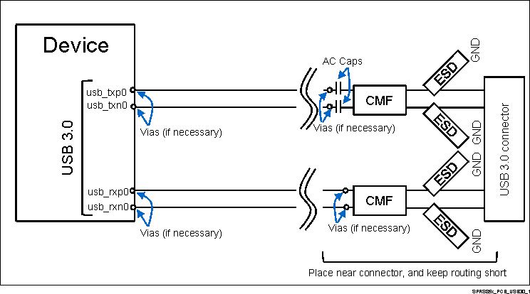
The USB 3.0 has two unidirectional differential pairs: TXp/TXn pair and RXp/RXn pair. AC coupling caps are needed on the board for TX traces.
Figure 7-39 present high level schematic diagram for USB 3.0 interface.
 Figure 7-39 USB 3.0 Interface High Level Schematic
 NOTE
ESD components should be on a PCB layer next to a system GND plane layer so the inductance of the via to GND will be minimal.
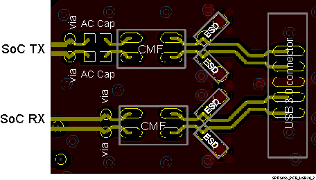
If vias are used, place the vias near the AC Caps or CMFs and under the SoC BGA, if necessary.
Figure 7-40 present placement diagram for USB 3.0 interface.
 Figure 7-40 USB 3.0 placement diagram
 Table 7-10 USB1 Component Reference
| INTERFACE | COMPONENT | SUPPLIER | PART NUMBER |
|---|---|---|---|
| USB3 PHY | ESD | TI | TPD1E05U06 |
| CMF | Murata | DLW21SN900HQ2 | |
| C | - | 100 nF (typical size: 0201) |