ZHCSH24G June 2016 – March 2019 TDA3LA , TDA3LX , TDA3MA , TDA3MD , TDA3MV
PRODUCTION DATA.
- 1 器件概述
- 2 修订历史记录
- 3 Device Comparison
-
4 Terminal Configuration and Functions
- 4.1 Terminal Assignment
- 4.2 Ball Characteristics
- 4.3 Multiplexing Characteristics
- 4.4
Signal Descriptions
- 4.4.1 Video Input Ports (VIP)
- 4.4.2 Display Subsystem – Video Output Ports
- 4.4.3 Digital-to-Analog Converter (SD_DAC)
- 4.4.4 Embedded 8 channel Analog-To-Digital Converter (ADC)
- 4.4.5 Camera Control
- 4.4.6 Camera Parallel Interface (CPI)
- 4.4.7 Imaging Subsystem (ISS)
- 4.4.8 External Memory Interface (EMIF)
- 4.4.9 General-Purpose Memory Controller (GPMC)
- 4.4.10 Timers
- 4.4.11 Inter-Integrated Circuit Interface (I2C)
- 4.4.12 Universal Asynchronous Receiver Transmitter (UART)
- 4.4.13 Multichannel Serial Peripheral Interface (McSPI)
- 4.4.14 Quad Serial Peripheral Interface (QSPI)
- 4.4.15 Multichannel Audio Serial Port (McASP)
- 4.4.16 Controller Area Network Interface (DCAN and MCAN)
- 4.4.17 Ethernet Interface (GMAC_SW)
- 4.4.18 SDIO Controller
- 4.4.19 General-Purpose Interface (GPIO)
- 4.4.20 Pulse Width Modulation (PWM) Interface
- 4.4.21 Test Interfaces
- 4.4.22 System and Miscellaneous
- 4.4.23 Power Supplies
-
5 Specifications
- 5.1 Absolute Maximum Ratings
- 5.2 ESD Ratings
- 5.3 Power On Hour (POH) Limits
- 5.4 Power on Hour (POH) Limits
- 5.5 Recommended Operating Conditions
- 5.6 Operating Performance Points
- 5.7 Power Consumption Summary
- 5.8
Electrical Characteristics
- 5.8.1 LVCMOS DDR DC Electrical Characteristics
- 5.8.2 Dual Voltage LVCMOS I2C DC Electrical Characteristics
- 5.8.3 IQ1833 Buffers DC Electrical Characteristics
- 5.8.4 IHHV1833 Buffers DC Electrical Characteristics
- 5.8.5 LVCMOS Analog OSC Buffers DC Electrical Characteristics
- 5.8.6 LVCMOS CSI2 DC Electrical Characteristics
- 5.8.7 Dual Voltage LVCMOS DC Electrical Characteristics
- 5.9 Thermal Characteristics
- 5.10 Analog-to-Digital ADC Subsystem Electrical Specifications
- 5.11 Power Supply Sequences
- 6 Clock Specifications
-
7 Timing Requirements and Switching Characteristics
- 7.1 Timing Test Conditions
- 7.2 Interface Clock Specifications
- 7.3 Timing Parameters and Information
- 7.4 Recommended Clock and Control Signal Transition Behavior
- 7.5 Video Input Ports (VIP)
- 7.6 Display Subsystem – Video Output Ports
- 7.7 Imaging Subsystem (ISS)
- 7.8 External Memory Interface (EMIF)
- 7.9 General-Purpose Memory Controller (GPMC)
- 7.10 General-Purpose Timers
- 7.11 Inter-Integrated Circuit Interface (I2C)
- 7.12 Universal Asynchronous Receiver Transmitter (UART)
- 7.13 Multichannel Serial Peripheral Interface (McSPI)
- 7.14 Quad Serial Peripheral Interface (QSPI)
- 7.15
Multichannel Audio Serial Port (McASP)
- Table 7-26 Timing Requirements for McASP1
- Table 7-27 Timing Requirements for McASP2
- Table 7-28 Timing Requirements for McASP3
- Table 7-29 Switching Characteristics Over Recommended Operating Conditions for McASP1
- Table 7-30 Switching Characteristics Over Recommended Operating Conditions for McASP2
- Table 7-31 Switching Characteristics Over Recommended Operating Conditions for McASP3
- 7.16 Controller Area Network Interface (DCAN and MCAN)
- 7.17
Ethernet Interface (GMAC_SW)
- 7.17.1 GMAC MDIO Interface Timings
- 7.17.2
GMAC RGMII Timings
- Table 7-39 Timing Requirements for rgmiin_rxc - RGMIIn Operation
- Table 7-40 Timing Requirements for GMAC RGMIIn Input Receive for 10/100/1000 Mbps
- Table 7-41 Switching Characteristics Over Recommended Operating Conditions for rgmiin_txctl - RGMIIn Operation for 10/100/1000 Mbit/s
- Table 7-42 Switching Characteristics for GMAC RGMIIn Output Transmit for 10/100/1000 Mbps
- 7.18 SDIO Controller
- 7.19 General-Purpose Interface (GPIO)
- 7.20
Test Interfaces
- 7.20.1
JTAG Electrical Data/Timing
- Table 7-53 Timing Requirements for IEEE 1149.1 JTAG
- Table 7-54 Switching Characteristics Over Recommended Operating Conditions for IEEE 1149.1 JTAG
- Table 7-55 Timing Requirements for IEEE 1149.1 JTAG With RTCK
- Table 7-56 Switching Characteristics Over Recommended Operating Conditions for IEEE 1149.1 JTAG With RTCK
- 7.20.2 Trace Port Interface Unit (TPIU)
- 7.20.1
JTAG Electrical Data/Timing
-
8 Applications, Implementation, and Layout
- 8.1 Introduction
- 8.2 Power Optimizations
- 8.3 Core Power Domains
- 8.4 Single-Ended Interfaces
- 8.5 Differential Interfaces
- 8.6 Clock Routing Guidelines
- 8.7 LPDDR2 Board Design and Layout Guidelines
- 8.8 DDR2 Board Design and Layout Guidelines
- 8.9
DDR3 Board Design and Layout Guidelines
- 8.9.1 DDR3 General Board Layout Guidelines
- 8.9.2
DDR3 Board Design and Layout Guidelines
- 8.9.2.1 Board Designs
- 8.9.2.2 DDR3 Device Combinations
- 8.9.2.3 DDR3 Interface Schematic
- 8.9.2.4 Compatible JEDEC DDR3 Devices
- 8.9.2.5 PCB Stackup
- 8.9.2.6 Placement
- 8.9.2.7 DDR3 Keepout Region
- 8.9.2.8 Bulk Bypass Capacitors
- 8.9.2.9 High-Speed Bypass Capacitors
- 8.9.2.10 Net Classes
- 8.9.2.11 DDR3 Signal Termination
- 8.9.2.12 VTT
- 8.9.2.13 CK and ADDR_CTRL Topologies and Routing Definition
- 8.9.2.14 Data Topologies and Routing Definition
- 8.9.2.15 Routing Specification
- 8.10 CVIDEO/SD-DAC Guidelines and Electrical Data/Timing
- 9 Device and Documentation Support
- 10Mechanical, Packaging, and Orderable Information
8.9.2.13.1.2 CK and ADDR_CTRL Routing, Three DDR3 Devices
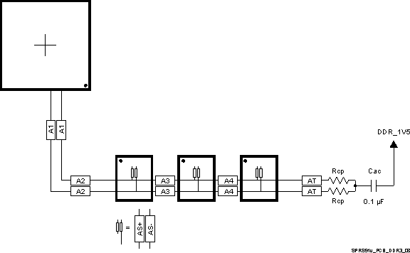
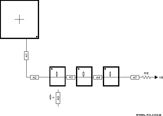
Figure 8-51 shows the CK routing for three DDR3 devices placed on the same side of the PCB. Figure 8-52 shows the corresponding ADDR_CTRL routing.
 Figure 8-51 CK Routing for Three Single-Side DDR3 Devices
  Figure 8-52 ADDR_CTRL Routing for Three Single-Side DDR3 Devices
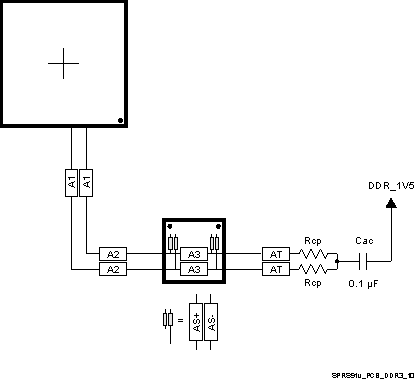
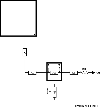
 To save PCB space, the two DDR3 memories may be mounted as one mirrored pair at a cost of increased routing and assembly complexity. Figure 8-53 and Figure 8-54 show the routing for CK and ADDR_CTRL, respectively, for two DDR3 devices mirrored in a pair configuration.
 Figure 8-53 CK Routing for Two Mirrored DDR3 Devices
  Figure 8-54 ADDR_CTRL Routing for Two Mirrored DDR3 Devices