ZHCSRF7A december 2022 – august 2023 TDA4AL-Q1 , TDA4VE-Q1 , TDA4VL-Q1
PRODUCTION DATA
- 1
- 1 特性
- 2 应用
- 3 说明
- 4 Revision History
- 5 Device Comparison
-
6 Terminal Configuration and Functions
- 6.1 Pin Diagrams
- 6.2 Pin Attributes
- 6.3
Signal Descriptions
- 14
- 6.3.1 ADC
- 6.3.2 DDRSS
- 6.3.3 GPIO
- 6.3.4 I2C
- 6.3.5 I3C
- 6.3.6 MCAN
- 6.3.7 MCSPI
- 6.3.8 UART
- 6.3.9 MDIO
- 6.3.10 CPSW2G
- 6.3.11 ECAP
- 6.3.12 EQEP
- 6.3.13 EPWM
- 6.3.14 USB
- 6.3.15 Display Port
- 6.3.16 Hyperlink
- 6.3.17 PCIE
- 6.3.18 SERDES
- 6.3.19 DSI
- 6.3.20 CSI
- 6.3.21 MCASP
- 6.3.22 DMTIMER
- 6.3.23 CPTS
- 6.3.24 DSS
- 6.3.25 GPMC
- 6.3.26 MMC
- 6.3.27 OSPI
- 6.3.28 Hyperbus
- 6.3.29 Emulation and Debug
- 6.3.30 System and Miscellaneous
- 6.3.31 Power
- 6.4 Connection for Unused Pins
-
7 Specifications
- 7.1 Absolute Maximum Ratings
- 7.2 ESD Ratings
- 7.3 Recommended Operating Conditions
- 7.4 Power-On-Hour (POH) Limits
- 7.5 Operating Performance Points
- 7.6
Electrical Characteristics
- 7.6.1 I2C, Open-Drain, Fail-Safe (I2C OD FS) Electrical Characteristics
- 7.6.2 Fail-Safe Reset (FS Reset) Electrical Characteristics
- 7.6.3 HFOSC/LFOSC Electrical Characteristics
- 7.6.4 eMMCPHY Electrical Characteristics
- 7.6.5 SDIO Electrical Characteristics
- 7.6.6 CSI2/DSI D-PHY Electrical Characteristics
- 7.6.7 ADC12B Electrical Characteristics
- 7.6.8 LVCMOS Electrical Characteristics
- 7.6.9 USB2PHY Electrical Characteristics
- 7.6.10 SerDes 2-L-PHY/4-L-PHY Electrical Characteristics
- 7.6.11 UFS M-PHY Electrical Characteristics
- 7.6.12 eDP/DP AUX-PHY Electrical Characteristics
- 7.6.13 DDR0 Electrical Characteristics
- 7.7 VPP Specifications for One-Time Programmable (OTP) eFuses
- 7.8 Thermal Resistance Characteristics
- 7.9 Temperature Sensor Characteristics
- 7.10
Timing and Switching Characteristics
- 7.10.1 Timing Parameters and Information
- 7.10.2
Power Supply Sequencing
- 7.10.2.1 Power Supply Slew Rate Requirement
- 7.10.2.2 Combined MCU and Main Domains Power- Up Sequencing
- 7.10.2.3 Combined MCU and Main Domains Power- Down Sequencing
- 7.10.2.4 Isolated MCU and Main Domains Power- Up Sequencing
- 7.10.2.5 Isolated MCU and Main Domains Power- Down Sequencing
- 7.10.2.6 Independent MCU and Main Domains, Entry and Exit of MCU Only Sequencing
- 7.10.2.7 Independent MCU and Main Domains, Entry and Exit of DDR Retention State
- 7.10.2.8 Independent MCU and Main Domains, Entry and Exit of GPIO Retention Sequencing
- 7.10.3 System Timing
- 7.10.4
Clock Specifications
- 7.10.4.1 Input and Output Clocks / Oscillators
- 7.10.4.2 Output Clocks
- 7.10.4.3 PLLs
- 7.10.4.4 Module and Peripheral Clocks Frequencies
- 7.10.5
Peripherals
- 7.10.5.1 ATL
- 7.10.5.2
CPSW2G
- 7.10.5.2.1 CPSW2G MDIO Interface Timings
- 7.10.5.2.2 CPSW2G RMII Timings
- 7.10.5.2.3
CPSW2G RGMII Timings
- 7.10.5.2.3.1 RGMII[x]_RXC Timing Requirements – RGMII Mode
- 7.10.5.2.3.2 CPSW2G Timing Requirements for RGMII[x]_RD[3:0], and RGMII[x]_RCTL – RGMII Mode
- 7.10.5.2.3.3 CPSW2G RGMII[x]_TXC Switching Characteristics – RGMII Mode
- 7.10.5.2.3.4 RGMII[x]_TD[3:0], and RGMII[x]_TX_CTL Switching Characteristics – RGMII Mode
- 7.10.5.3 CSI-2
- 7.10.5.4 DDRSS
- 7.10.5.5 DSS
- 7.10.5.6 eCAP
- 7.10.5.7 EPWM
- 7.10.5.8 eQEP
- 7.10.5.9 GPIO
- 7.10.5.10 GPMC
- 7.10.5.11 HyperBus
- 7.10.5.12 I2C
- 7.10.5.13 I3C
- 7.10.5.14 MCAN
- 7.10.5.15 MCASP
- 7.10.5.16 MCSPI
- 7.10.5.17 MMCSD
- 7.10.5.18 CPTS
- 7.10.5.19 OSPI
- 7.10.5.20 PCIE
- 7.10.5.21 Timers
- 7.10.5.22 UART
- 7.10.5.23 USB
- 7.10.6 Emulation and Debug
-
8 Applications,
Implementation, and Layout
- 8.1 Device Connection and Layout Fundamentals
- 8.2 Peripheral- and Interface-Specific Design Information
- 9 Device and Documentation Support
- 10Mechanical, Packaging, and Orderable Information
7.10.4.1.3.1 Load Capacitance
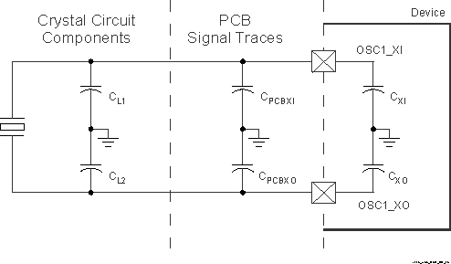
The crystal circuit must be designed such that it applies the appropriate capacitive load to the crystal, as defined by the crystal manufacturer. The capacitive load, CL, of this circuit is a combination of discrete capacitors CL1, CL2, and several parasitic contributions. PCB signal traces which connect crystal circuit components to OSC1_XI and OSC1_XO have parasitic capacitance to ground, CPCBXI and CPCBXO, where the PCB designer should be able to extract parasitic capacitance for each signal trace. The OSC1 circuits and device package have combined parasitic capacitance to ground, CPCBXI and CPCBXO, where these parasitic capacitance values are defined in Table 7-24.
 Figure 7-30 Load Capacitance
Load capacitors, CL1 and CL2 in Figure 7-28, should be chosen such that the below equation is satisfied. CL in the equation is the load specified by the crystal manufacturer.
CL = [(CL1 + CPCBXI + CXI) × (CL2 + CPCBXO + CXO)] / [(CL1 + CPCBXI + CXI) + (CL2 + CPCBXO + CXO)]
To determine the value of CL1 and CL2, multiply the capacitive load value CL by 2. Using this result, subtract the combined values of CPCBXI + CXI to determine the value of CL1 and the combined values of CPCBXO + CXO to determine the value of CL2. For example, if CL = 10 pF, CPCBXI = 2.9 pF, CXI = 0.5 pF, CPCBXO = 3.7 pF, CXO = 0.5 pF, the value of CL1 = [(2CL) - (CPCBXI + CXI)] = [(2 × 10 pF) - 2.9 pF - 0.5 pF)] = 16.6 pF and CL2 = [(2CL) - (CPCBXO + CXO)] = [(2 × 10 pF) - 3.7 pF - 0.5 pF)] = 15.8 pF