ZHCSKP3K September 2021 – April 2024 TDA4VM , TDA4VM-Q1
PRODUCTION DATA
- 1
- 1 特性
- 2 应用
- 3 说明
- 4 Device Comparison
-
5 Terminal Configuration and Functions
- 5.1 Pin Diagram
- 5.2 Pin Attributes
- 5.3
Signal Descriptions
- 5.3.1 ADC
- 5.3.2 DDRSS
- 5.3.3 GPIO
- 5.3.4 I2C
- 5.3.5 I3C
- 5.3.6 MCAN
- 5.3.7 MCSPI
- 5.3.8 UART
- 5.3.9 MDIO
- 5.3.10 CPSW2G
- 5.3.11 CPSW9G
- 5.3.12 ECAP
- 5.3.13 EQEP
- 5.3.14 EHRPWM
- 5.3.15 USB
- 5.3.16 SERDES
- 5.3.17 OSPI
- 5.3.18 Hyperbus
- 5.3.19 GPMC
- 5.3.20 MMC
- 5.3.21 CPTS
- 5.3.22 UFS
- 5.3.23 PRU_ICSSG [Currently Not Supported]
- 5.3.24 MCASP
- 5.3.25 DSS
- 5.3.26 DP
- 5.3.27 Camera Streaming Interface Receiver (CSI_RX_IF) Subsystem
- 5.3.28 DSI_TX
- 5.3.29 VPFE
- 5.3.30 DMTIMER
- 5.3.31 Emulation and Debug
- 5.3.32 System and Miscellaneous
- 5.3.33 Power Supply
- 5.4 Pin Multiplexing
- 5.5 Pin Connectivity Requirements
-
6 Specifications
- 6.1 Absolute Maximum Ratings
- 6.2 ESD Ratings
- 6.3 Power-On-Hour (POH) Limits
- 6.4 Recommended Operating Conditions
- 6.5 Operating Performance Points
- 6.6 Electrical Characteristics
- 6.7 VPP Specifications for One-Time Programmable (OTP) eFuses
- 6.8 Thermal Resistance Characteristics
- 6.9
Timing and Switching Characteristics
- 6.9.1 Timing Parameters and Information
- 6.9.2
Power Supply Sequencing
- 6.9.2.1 Power Supply Slew Rate Requirement
- 6.9.2.2 Combined MCU and Main Domains Power-Up Sequencing
- 6.9.2.3 Combined MCU and Main Domains Power- Down Sequencing
- 6.9.2.4 Isolated MCU and Main Domains Power- Up Sequencing
- 6.9.2.5 Isolated MCU and Main Domains, Primary Power- Down Sequencing
- 6.9.2.6 Entry and Exit of MCU Only State
- 6.9.2.7 Entry and Exit of DDR Retention State
- 6.9.3 System Timing
- 6.9.4
Clock Specifications
- 6.9.4.1
Input and Output Clocks / Oscillators
- 6.9.4.1.1 WKUP_OSC0 Internal Oscillator Clock Source
- 6.9.4.1.2 WKUP_OSC0 LVCMOS Digital Clock Source
- 6.9.4.1.3 Auxiliary OSC1 Internal Oscillator Clock Source
- 6.9.4.1.4 Auxiliary OSC1 LVCMOS Digital Clock Source
- 6.9.4.1.5 Auxiliary OSC1 Not Used
- 6.9.4.1.6 WKUP_LFOSC0 Internal Oscillator Clock Source
- 6.9.4.1.7 WKUP_LFOSC0 Not Used
- 6.9.4.2 Output Clocks
- 6.9.4.3 PLLs
- 6.9.4.4 Module and Peripheral Clocks Frequencies
- 6.9.4.1
Input and Output Clocks / Oscillators
- 6.9.5
Peripherals
- 6.9.5.1 ATL
- 6.9.5.2 VPFE
- 6.9.5.3
CPSW2G
- 6.9.5.3.1 CPSW2G MDIO Interface Timings
- 6.9.5.3.2 CPSW2G RMII Timings
- 6.9.5.3.3
CPSW2G RGMII Timings
- 6.9.5.3.3.1 RGMII[x]_RXC Timing Requirements – RGMII Mode
- 6.9.5.3.3.2 CPSW2G Timing Requirements for RGMII[x]_RD[3:0], and RGMII[x]_RCTL – RGMII Mode
- 6.9.5.3.3.3 CPSW2G RGMII[x]_TXC Switching Characteristics – RGMII Mode
- 6.9.5.3.3.4 RGMII[x]_TD[3:0], and RGMII[x]_TX_CTL Switching Characteristics – RGMII Mode
- 6.9.5.4 CPSW9G
- 6.9.5.5 CSI-2
- 6.9.5.6 DDRSS
- 6.9.5.7 DSS
- 6.9.5.8 eCAP
- 6.9.5.9 EPWM
- 6.9.5.10 eQEP
- 6.9.5.11 GPIO
- 6.9.5.12 GPMC
- 6.9.5.13 HyperBus
- 6.9.5.14 I2C
- 6.9.5.15 I3C
- 6.9.5.16 MCAN
- 6.9.5.17 MCASP
- 6.9.5.18 MCSPI
- 6.9.5.19 MMCSD
- 6.9.5.20 CPTS
- 6.9.5.21 OSPI
- 6.9.5.22 PCIE
- 6.9.5.23 Timers
- 6.9.5.24 UART
- 6.9.5.25 USB
- 6.9.6 Emulation and Debug
-
7 Detailed Description
- 7.1 Overview
- 7.2 Processor Subsystems
- 7.3 Accelerators and Coprocessors
- 7.4
Other Subsystems
- 7.4.1 MSMC
- 7.4.2 NAVSS
- 7.4.3 PDMA Controller
- 7.4.4 Power Supply
- 7.4.5
Peripherals
- 7.4.5.1 ADC
- 7.4.5.2 ATL
- 7.4.5.3 CSI
- 7.4.5.4 CPSW2G
- 7.4.5.5 CPSW9G
- 7.4.5.6 DCC
- 7.4.5.7 DDRSS
- 7.4.5.8 DSS
- 7.4.5.9 VPFE
- 7.4.5.10 eCAP
- 7.4.5.11 EPWM
- 7.4.5.12 ELM
- 7.4.5.13 ESM
- 7.4.5.14 eQEP
- 7.4.5.15 GPIO
- 7.4.5.16 GPMC
- 7.4.5.17 Hyperbus
- 7.4.5.18 I2C
- 7.4.5.19 I3C
- 7.4.5.20 MCAN
- 7.4.5.21 MCASP
- 7.4.5.22 MCRC Controller
- 7.4.5.23 MCSPI
- 7.4.5.24 MMC/SD
- 7.4.5.25 OSPI
- 7.4.5.26 PCIE
- 7.4.5.27 SerDes
- 7.4.5.28 WWDT
- 7.4.5.29 Timers
- 7.4.5.30 UART
- 7.4.5.31 USB
- 7.4.5.32 UFS
-
8 Applications and
Implementation
- 8.1 Power Supply Mapping
- 8.2 Device Connection and Layout Fundamentals
- 8.3
Peripheral- and Interface-Specific Design Information
- 8.3.1 LPDDR4 Board Design and Layout Guidelines
- 8.3.2 OSPI and QSPI Board Design and Layout Guidelines
- 8.3.3 SERDES REFCLK Design Guidelines
- 8.3.4 USB VBUS Design Guidelines
- 8.3.5 System Power Supply Monitor Design Guidelines
- 8.3.6 High Speed Differential Signal Routing Guidance
- 8.3.7 Thermal Solution Guidance
- 9 Device and Documentation Support
- 10Revision History
- 11Mechanical, Packaging, and Orderable Information
6.9.4.1.3.2 Shunt Capacitance
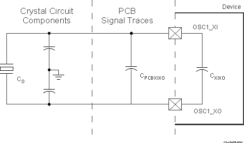
The crystal circuit must also be designed such that it does not exceed the maximum shunt capacitance for OSC1 operating conditions defined in Table 6-31. Shunt capacitance, Cshunt, of the crystal circuit is a combination of crystal shunt capacitance and parasitic contributions. PCB signal traces which connect crystal circuit components to OSC1 have mutual parasitic capacitance to each other, CPCBXIXO, where the PCB designer should be able to extract mutual parasitic capacitance between these signal traces. The device package also has mutual parasitic capacitance, CXIXO, where this mutual parasitic capacitance value is defined in Table 6-32.
PCB routing should be designed to minimize mutual capacitance between XI and XO signal traces. This is typically done by keeping signal traces short and not routing them in close proximity. Mutual capacitance can also be minimized by placing a ground trace between these signals when the layout requires them to be routed in close proximity. It is important to minimize the mutual capacitance on the PCB to provide as much margin as possible when selecting a crystal.
 Figure 6-31 Shunt Capacitance
A crystal should be chosen such that the below equation is satisfied. CO in the equation is the maximum shunt capacitance specified by the crystal manufacturer.
Cshunt ≥ CO + CPCBXIXO + CXIXO
For example, the equation would be satisfied when the crystal being used is 25 MHz with an ESR = 30 Ω, CPCBXIXO = 0.04 pF, CXIXO = 0.01 pF, and shunt capacitance of the crystal is less than or equal to 6.95 pF.