ZHCSRW2A february 2023 – august 2023 TDA4AH-Q1 , TDA4AP-Q1 , TDA4VH-Q1 , TDA4VP-Q1
ADVANCE INFORMATION
- 1
- 1 特性
- 2 应用
- 3 说明
- 4 Revision History
- 5 Device Comparison
-
6 Terminal Configuration and Functions
- 6.1 Pin Diagrams
- 6.2 Pin Attributes
- 6.3
Signal Descriptions
- 14
- 6.3.1 ADC
- 6.3.2 DDRSS
- 6.3.3 GPIO
- 6.3.4 I2C
- 6.3.5 I3C
- 6.3.6 MCAN
- 6.3.7 MCSPI
- 6.3.8 UART
- 6.3.9 MDIO
- 6.3.10 UFS
- 6.3.11 CPSW2G
- 6.3.12 SGMII
- 6.3.13 ECAP
- 6.3.14 EQEP
- 6.3.15 EPWM
- 6.3.16 USB
- 6.3.17 Display Port
- 6.3.18 Hyperlink
- 6.3.19 PCIE
- 6.3.20 SERDES
- 6.3.21 DSI
- 6.3.22 CSI
- 6.3.23 MCASP
- 6.3.24 DMTIMER
- 6.3.25 CPTS
- 6.3.26 DSS
- 6.3.27 GPMC
- 6.3.28 MMC
- 6.3.29 OSPI
- 6.3.30 Hyperbus
- 6.3.31 Emulation and Debug
- 6.3.32 System and Miscellaneous
- 6.3.33 Power
- 6.4 Pin Connectivity Requirements
-
7 Specifications
- 7.1 Absolute Maximum Ratings
- 7.2 ESD Ratings
- 7.3 Power-On-Hour (POH) Limits
- 7.4 Recommended Operating Conditions
- 7.5 Operating Performance Points
- 7.6
Electrical Characteristics
- 7.6.1 I2C, Open-Drain, Fail-Safe (I2C OD FS) Electrical Characteristics
- 7.6.2 Fail-Safe Reset (FS Reset) Electrical Characteristics
- 7.6.3 HFOSC/LFOSC Electrical Characteristics
- 7.6.4 eMMCPHY Electrical Characteristics
- 7.6.5 SDIO Electrical Characteristics
- 7.6.6 CSI2/DSI D-PHY Electrical Characteristics
- 7.6.7 ADC12B Electrical Characteristics
- 7.6.8 LVCMOS Electrical Characteristics
- 7.6.9 USB2PHY Electrical Characteristics
- 7.6.10 SerDes 2-L-PHY/4-L-PHY Electrical Characteristics
- 7.6.11 UFS M-PHY Electrical Characteristics
- 7.6.12 eDP/DP AUX-PHY Electrical Characteristics
- 7.6.13 DDR0 Electrical Characteristics
- 7.7 VPP Specifications for One-Time Programmable (OTP) eFuses
- 7.8 Thermal Resistance Characteristics
- 7.9 Temperature Sensor Characteristics
- 7.10
Timing and Switching Characteristics
- 7.10.1 Timing Parameters and Information
- 7.10.2
Power Supply Sequencing
- 7.10.2.1 Power Supply Slew Rate Requirement
- 7.10.2.2 Combined MCU and Main Domains Power- Up Sequencing
- 7.10.2.3 Combined MCU and Main Domains Power- Down Sequencing
- 7.10.2.4 Isolated MCU and Main Domains Power- Up Sequencing
- 7.10.2.5 Isolated MCU and Main Domains Power- Down Sequencing
- 7.10.2.6 Independent MCU and Main Domains, Entry and Exit of MCU Only Sequencing
- 7.10.2.7 Independent MCU and Main Domains, Entry and Exit of DDR Retention State
- 7.10.2.8 Independent MCU and Main Domains, Entry and Exit of GPIO Retention Sequencing
- 7.10.3 System Timing
- 7.10.4
Clock Specifications
- 7.10.4.1 Input and Output Clocks / Oscillators
- 7.10.4.2 Output Clocks
- 7.10.4.3 PLLs
- 7.10.4.4 Module and Peripheral Clocks Frequencies
- 7.10.5
Peripherals
- 7.10.5.1 ATL
- 7.10.5.2
CPSW2G
- 7.10.5.2.1 CPSW2G MDIO Interface Timings
- 7.10.5.2.2 CPSW2G RMII Timings
- 7.10.5.2.3
CPSW2G RGMII Timings
- 7.10.5.2.3.1 RGMII[x]_RXC Timing Requirements – RGMII Mode
- 7.10.5.2.3.2 CPSW2G Timing Requirements for RGMII[x]_RD[3:0], and RGMII[x]_RCTL – RGMII Mode
- 7.10.5.2.3.3 CPSW2G RGMII[x]_TXC Switching Characteristics – RGMII Mode
- 7.10.5.2.3.4 RGMII[x]_TD[3:0], and RGMII[x]_TX_CTL Switching Characteristics – RGMII Mode
- 7.10.5.3 CSI-2
- 7.10.5.4 DDRSS
- 7.10.5.5 DSS
- 7.10.5.6 eCAP
- 7.10.5.7 EPWM
- 7.10.5.8 eQEP
- 7.10.5.9 GPIO
- 7.10.5.10 GPMC
- 7.10.5.11 HyperBus
- 7.10.5.12 I2C
- 7.10.5.13 I3C
- 7.10.5.14 MCAN
- 7.10.5.15 MCASP
- 7.10.5.16 MCSPI
- 7.10.5.17 MMCSD
- 7.10.5.18 CPTS
- 7.10.5.19 OSPI
- 7.10.5.20 OLDI
- 7.10.5.21 PCIE
- 7.10.5.22 Timers
- 7.10.5.23 UART
- 7.10.5.24 USB
- 7.10.6 Emulation and Debug
-
8 Detailed Description
- 8.1 Overview
- 8.2 Processor Subsystems
- 8.3 Accelerators and Coprocessors
- 8.4
Other Subsystems
- 8.4.1 MSMC
- 8.4.2 NAVSS
- 8.4.3 PDMA Controller
- 8.4.4 Power Supply
- 8.4.5
Peripherals
- 8.4.5.1 ADC
- 8.4.5.2 ATL
- 8.4.5.3 CSI
- 8.4.5.4 CPSW2G
- 8.4.5.5 CPSW9G
- 8.4.5.6 DCC
- 8.4.5.7 DDRSS
- 8.4.5.8 DSS
- 8.4.5.9 VPFE
- 8.4.5.10 eCAP
- 8.4.5.11 EPWM
- 8.4.5.12 ELM
- 8.4.5.13 ESM
- 8.4.5.14 eQEP
- 8.4.5.15 GPIO
- 8.4.5.16 GPMC
- 8.4.5.17 Hyperbus
- 8.4.5.18 I2C
- 8.4.5.19 I3C
- 8.4.5.20 MCAN
- 8.4.5.21 MCASP
- 8.4.5.22 MCRC Controller
- 8.4.5.23 MCSPI
- 8.4.5.24 MMC/SD
- 8.4.5.25 OSPI
- 8.4.5.26 PCIE
- 8.4.5.27 SerDes
- 8.4.5.28 WWDT
- 8.4.5.29 Timers
- 8.4.5.30 UART
- 8.4.5.31 USB
- 8.4.5.32 UFS
-
9 Applications,
Implementation, and Layout
- 9.1 Device Connection and Layout Fundamentals
- 9.2 Peripheral- and Interface-Specific Design Information
- 10Device and Documentation Support
- 11Mechanical, Packaging, and Orderable Information
7.10.3.1 Reset Timing
The tables and figures provided in this section define the timing requirements and switching characteristics for reset related signals.
Table 7-6 MCU_PORz Timing Requirements see Figure 7-10
| NO. | MIN | TYP | MAX | UNIT | ||
|---|---|---|---|---|---|---|
| RST1 | th(MCUD_SUPPLIES_VALID - MCU_PORz) | Hold time, MCU_PORz active (low) at Power-up after all MCU DOMAIN supplies valid (using external crystal) | N + 1200(2) | 9500000 | ns | |
| RST2 | Hold time, MCU_PORz active (low) at Power-up after all MCU DOMAIN supplies(1) valid and external clock stable (using external LVCMOS oscillator) | 1200 | ns | |||
| RST3 | tw(MCU_PORzL) | Pulse Width minimum, MCU_PORz low after Power-up (without removal of Power or system reference clock MCU_OSC0_XI/XO) | 1200 | ns | ||
(1) For the definition of the MCU DOMAIN supplies,
see the Section 7.10.2.2, Combined MCU and Main Domains Poewr-Up Sequencing.
(2) N = oscillator start-up time
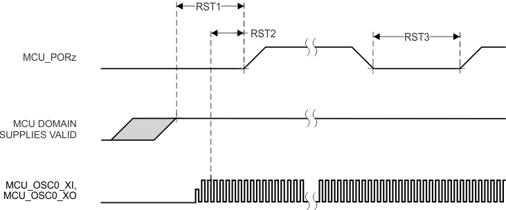 Figure 7-10 MCU_PORz Timing Requirements
 Table 7-7 PORz Timing Requirements see Figure 7-11
| NO. | MIN | MAX | UNIT | ||
|---|---|---|---|---|---|
| RST4 | th(MAIND_SUPPLIES_VALID - PORz) | Hold time, PORz active (low) at Power-up after all MAIN DOMAIN supplies(1) valid | 1200 | ns | |
| RST5 | tw(PORzL) | Pulse Width minimum, PORz low after Power-up | 1200 | ns | |
(1) For the definition of the
MAIN DOMAIN supplies, see the Section 7.10.2.2, Combined MCU and Main Domains Poewr-Up Sequencing.
 Figure 7-11 PORz Timing Requirements
Table 7-8 MCU_PORz initiates; MCU_PORz_OUT,
PORz_OUT, MCU_RESETSTATz, and RESETSTATz Switching Characteristics see Figure 7-12
| NO. | PARAMETER | MODE | MIN | MAX | UNIT | |
|---|---|---|---|---|---|---|
| RST6 | td(MCU_PORzL-MCU_PORz_OUTL) | Delay time, MCU_PORz active (low) to MCU_PORz_OUT active (low) | 0 | ns | ||
| RST7 | td(MCU_PORzH-MCU_PORz_OUTH) | Delay time, MCU_PORz inactive (high) to MCU_PORz_OUT inactive (high) | 0 | ns | ||
| RST8 | td(MCU_PORzL-PORz_OUTL) | Delay time, MCU_PORz active (low) to PORz_OUT active (low) | 0 | ns | ||
| RST9 | td(MCU_PORzH-PORz_OUTH) | Delay time, MCU_PORz inactive (high) to PORz_OUT inactive (high) | 1500 | ns | ||
| RST10 | td(MCU_PORzL-MCU_RESETSTATzL) | Delay time, MCU_PORz active (low) to MCU_RESETSTATz active (low) | 0 | ns | ||
| RST11 | td(MCU_PORzH-MCU_RESETSTATzH) | Delay time, MCU_PORz inactive (high) to MCU_RESETSTATz inactive (high) | POST bypass | 12000*S(1) | ns | |
| RST12 | td(MCU_PORzL-RESETSTATzL) | Delay time, MCU_PORz active (low) to RESETSTATz active (low) | 0 | ns | ||
| RST13 | td(MCU_PORzH-RESETSTATzH) | Delay time, MCU_PORz inactive (high) to RESETSTATz inactive (high) | 14500*S(1) | ns | ||
| RST14 | tw(MCU_PORz_OUTL) | Pulse width minimum, MCU_PORz_OUT active (low) | 1200 | ns | ||
| RST15 | tw(PORz_OUTL) | Pulse Width Minimum PORz_OUT low | 2550 | ns | ||
| RST16 | tw(MCU_RESETSTATzL) | Pulse Width Minimum MCU_RESETSTATz low | 3900*S(1) | ns | ||
| RST17 | tw(RESETSTATzL) | Pulse Width Minimum RESETSTATz low | 2650*S(1) | ns | ||
(1) S = MCU_OSC0_XI/XO clock period.
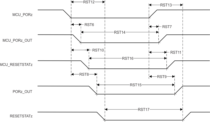 Figure 7-12 MCU_PORz initiates; MCU_PORz_OUT,
PORz_OUT, MCU_RESETSTATz, and RESETSTATz Switching Characteristics
Figure 7-12 MCU_PORz initiates; MCU_PORz_OUT,
PORz_OUT, MCU_RESETSTATz, and RESETSTATz Switching CharacteristicsTable 7-9 PORz Initiates; PORz_OUT and
RESETSTATz Switching Characteristics see Figure 7-13
| NO. | PARAMETER | MODE | MIN | MAX | UNIT | |
|---|---|---|---|---|---|---|
| RST18 | td(PORzL-PORz_OUTL) | Delay time, PORz active (low) toPORz_OUT active (low) | software control of POR_RST_ISO_DONE_Z | T(1) | ||
| CTRLMMR_WKUP_POR_RST _CTRL[0].POR_RST_ISO_ DONE_Z = 0 | 0 | ns | ||||
| RST19 | td(PORzH-PORz_OUTH) | Delay time, PORz active (high) toPORz_OUT active (high) | 1300 | ns | ||
| RST20 | td(PORzL-RESETSTATzL) | Delay time, PORz active (low) to RESETSTATz active (low) | T(1) | |||
| CTRLMMR_WKUP_POR_RST _CTRL[0].POR_RST_ISO_ DONE_Z = 0 | 0 | ns | ||||
| RST21 | td(PORzH-RESETSTATzH) | Delay time, PORz active (high) to RESETSTATz active (high) | 14500*S(2) | ns | ||
(1) T = Reset Isolation Time (Software
Dependent).
(2) S = MCU_OSC0_XI/XO clock period.
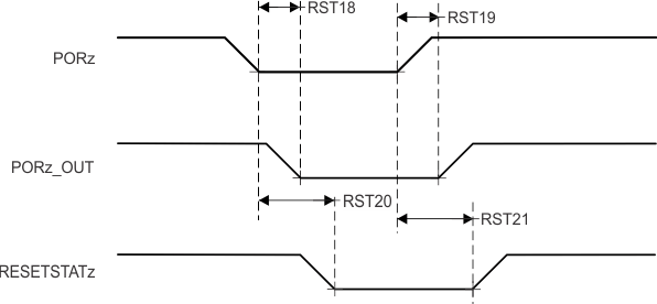 Figure 7-13 PORz initiates; PORz_OUT and
RESETSTATz Switching Characteristics
Figure 7-13 PORz initiates; PORz_OUT and
RESETSTATz Switching CharacteristicsTable 7-10 MCU_RESETz Timing Requirements see Figure 7-14
| NO. | MIN | MAX | UNIT | ||
|---|---|---|---|---|---|
| RST22 | tw(MCU_RESETzL)(1) | Pulse Width minimum, MCU_RESETz active (low) | 1200 | ns | |
(1) Timing for MCU_RESETz is valid only after
all supplies are valid and MCU_PORz has been asserted for the specified time.
Table 7-11 MCU_RESETz initiates; MCU_RESETSTATz,
and RESETSTATz Switching Characteristics see Figure 7-14
| NO. | PARAMETER | MIN | MAX | UNIT | |
|---|---|---|---|---|---|
| RST23 | td(MCU_RESETzL-MCU_RESETSTATzL) | Delay time, MCU_RESETz active (low) to MCU_RESETSTATz active (low) | 800 | ns | |
| RST24 | td(MCU_RESETzH-MCU_RESETSTATzH) | Delay time, MCU_RESETz inactive (high) to MCU_RESETSTATz inactive (high) | 3900*S(1) | ns | |
| RST25 | td(MCU_RESETzL-RESETSTATzL) | Delay time, MCU_RESETz active (low) to RESETSTATz active (low) | 800 | ns | |
| RST26 | td(MCU_RESETzH-RESETSTATzH) | Delay time, MCU_RESETz inactive (high) to RESETSTATz inactive (high) | 3900*S(1) | ns | |
(1) S = MCU_OSC0_XI/XO clock period.
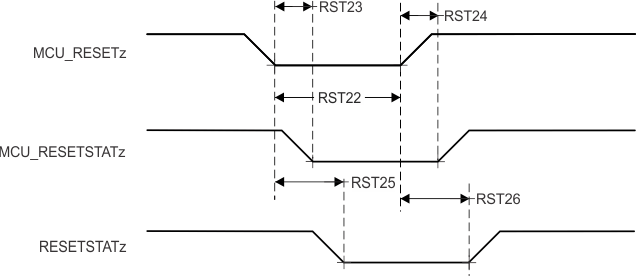 Figure 7-14 MCU_RESETz initiates; MCU_RESETSTATz,
and RESETSTATz Timing Requirements and Switching Characteristics
Figure 7-14 MCU_RESETz initiates; MCU_RESETSTATz,
and RESETSTATz Timing Requirements and Switching CharacteristicsTable 7-12 RESET_REQz Timing Requirements see Figure 7-15
| NO. | MIN | MAX | UNIT | ||
|---|---|---|---|---|---|
| RST27 | tw(RESET_REQzL)(1) | Pulse Width minimum, RESET_REQz active (low) | 1200 | ns | |
(1) Timing for RESET_REQz is valid only after
all supplies are valid and MCU_PORz has been asserted for the specified time.
Table 7-13 RESET_REQz initiates; RESETSTATz
Switching Characteristics see Figure 7-15
| NO. | PARAMETER | MODE | MIN | MAX | UNIT | |
|---|---|---|---|---|---|---|
| RST28 | td(RESET_REQzL-RESETSTATzL) | Delay time, RESET_REQz active (low) to RESETSTATz active (low) | software control of SOC_WARMRST_ISO_DONE_Z | T(1) | ||
| CTRLMMR_WKUP_MAIN_WARM _RST_CTRL[0].SOC_ WARMRST_ISO_DONE_Z = 0 | 740 | ns | ||||
| RST29 | td(RESET_REQzH-RESETSTATzH) | Delay time, RESET_REQz inactive (high) to RESETSTATz inactive (high) | 2650*S(2) | ns | ||
(1) T = Reset Isolation Time (Software
Dependent).
(2) S = MCU_OSC0_XI/XO clock period.
 Figure 7-15 RESET_REQz initiates; RESETSTATz
Timing Requirements and Switching Characteristics
Figure 7-15 RESET_REQz initiates; RESETSTATz
Timing Requirements and Switching CharacteristicsTable 7-14 EMUx Timing Requirements see Figure 7-16
| NO. | MIN | MAX | UNIT | ||
|---|---|---|---|---|---|
| RST30 | tsu(EMUx-MCU_PORz) | Setup time, EMU[1:0] before MCU_PORz inactive (high) | 3*S(1) | ns | |
| RST31 | th(MCU_PORz - EMUx) | Hold time, EMU[1:0] after MCU_PORz inactive (high) | 10 | ns | |
(1) S = MCU_OSC0_XI/XO clock period.
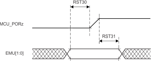 Figure 7-16 EMUx Timing Requirements
Table 7-15 MCU_BOOTMODE Timing
Requirements see Figure 7-17
| NO. | MIN | MAX | UNIT | ||
|---|---|---|---|---|---|
| RST32 | tsu(MCU_BOOTMODE-MCU_PORz_OUT) | Setup time, MCU_BOOTMODE[09:00] before MCU_PORz_OUT high | 3*S(1) | ns | |
| RST33 | th(MCU_PORz_OUT - MCU_BOOTMODE) | Hold time, MCU_BOOTMODE[09:00] after MCU_ PORz_OUT high | 0 | ns | |
(1) S = MCU_OSC0_XI/XO clock period.
 Figure 7-17 MCU_BOOTMODE
Timing Requirements
Figure 7-17 MCU_BOOTMODE
Timing RequirementsTable 7-16 BOOTMODE Timing Requirements see Figure 7-18
| NO. | MIN | MAX | UNIT | ||
|---|---|---|---|---|---|
| RST34 | tsu(BOOTMODE-PORz_OUT) | Setup time, BOOTMODE[7:0] before PORz_OUT high | 3*S(1) | ns | |
| RST35 | th(PORz_OUT - BOOTMODE) | Hold time, BOOTMODE[7:0] after PORz_OUT high | 0 | ns | |
(1) S = MCU_OSC0_XI/XO clock period.
 Figure 7-18 BOOTMODE Timing
Requirements