ZHCSRW2A february 2023 – august 2023 TDA4AH-Q1 , TDA4AP-Q1 , TDA4VH-Q1 , TDA4VP-Q1
ADVANCE INFORMATION
- 1
- 1 特性
- 2 应用
- 3 说明
- 4 Revision History
- 5 Device Comparison
-
6 Terminal Configuration and Functions
- 6.1 Pin Diagrams
- 6.2 Pin Attributes
- 6.3
Signal Descriptions
- 14
- 6.3.1 ADC
- 6.3.2 DDRSS
- 6.3.3 GPIO
- 6.3.4 I2C
- 6.3.5 I3C
- 6.3.6 MCAN
- 6.3.7 MCSPI
- 6.3.8 UART
- 6.3.9 MDIO
- 6.3.10 UFS
- 6.3.11 CPSW2G
- 6.3.12 SGMII
- 6.3.13 ECAP
- 6.3.14 EQEP
- 6.3.15 EPWM
- 6.3.16 USB
- 6.3.17 Display Port
- 6.3.18 Hyperlink
- 6.3.19 PCIE
- 6.3.20 SERDES
- 6.3.21 DSI
- 6.3.22 CSI
- 6.3.23 MCASP
- 6.3.24 DMTIMER
- 6.3.25 CPTS
- 6.3.26 DSS
- 6.3.27 GPMC
- 6.3.28 MMC
- 6.3.29 OSPI
- 6.3.30 Hyperbus
- 6.3.31 Emulation and Debug
- 6.3.32 System and Miscellaneous
- 6.3.33 Power
- 6.4 Pin Connectivity Requirements
-
7 Specifications
- 7.1 Absolute Maximum Ratings
- 7.2 ESD Ratings
- 7.3 Power-On-Hour (POH) Limits
- 7.4 Recommended Operating Conditions
- 7.5 Operating Performance Points
- 7.6
Electrical Characteristics
- 7.6.1 I2C, Open-Drain, Fail-Safe (I2C OD FS) Electrical Characteristics
- 7.6.2 Fail-Safe Reset (FS Reset) Electrical Characteristics
- 7.6.3 HFOSC/LFOSC Electrical Characteristics
- 7.6.4 eMMCPHY Electrical Characteristics
- 7.6.5 SDIO Electrical Characteristics
- 7.6.6 CSI2/DSI D-PHY Electrical Characteristics
- 7.6.7 ADC12B Electrical Characteristics
- 7.6.8 LVCMOS Electrical Characteristics
- 7.6.9 USB2PHY Electrical Characteristics
- 7.6.10 SerDes 2-L-PHY/4-L-PHY Electrical Characteristics
- 7.6.11 UFS M-PHY Electrical Characteristics
- 7.6.12 eDP/DP AUX-PHY Electrical Characteristics
- 7.6.13 DDR0 Electrical Characteristics
- 7.7 VPP Specifications for One-Time Programmable (OTP) eFuses
- 7.8 Thermal Resistance Characteristics
- 7.9 Temperature Sensor Characteristics
- 7.10
Timing and Switching Characteristics
- 7.10.1 Timing Parameters and Information
- 7.10.2
Power Supply Sequencing
- 7.10.2.1 Power Supply Slew Rate Requirement
- 7.10.2.2 Combined MCU and Main Domains Power- Up Sequencing
- 7.10.2.3 Combined MCU and Main Domains Power- Down Sequencing
- 7.10.2.4 Isolated MCU and Main Domains Power- Up Sequencing
- 7.10.2.5 Isolated MCU and Main Domains Power- Down Sequencing
- 7.10.2.6 Independent MCU and Main Domains, Entry and Exit of MCU Only Sequencing
- 7.10.2.7 Independent MCU and Main Domains, Entry and Exit of DDR Retention State
- 7.10.2.8 Independent MCU and Main Domains, Entry and Exit of GPIO Retention Sequencing
- 7.10.3 System Timing
- 7.10.4
Clock Specifications
- 7.10.4.1 Input and Output Clocks / Oscillators
- 7.10.4.2 Output Clocks
- 7.10.4.3 PLLs
- 7.10.4.4 Module and Peripheral Clocks Frequencies
- 7.10.5
Peripherals
- 7.10.5.1 ATL
- 7.10.5.2
CPSW2G
- 7.10.5.2.1 CPSW2G MDIO Interface Timings
- 7.10.5.2.2 CPSW2G RMII Timings
- 7.10.5.2.3
CPSW2G RGMII Timings
- 7.10.5.2.3.1 RGMII[x]_RXC Timing Requirements – RGMII Mode
- 7.10.5.2.3.2 CPSW2G Timing Requirements for RGMII[x]_RD[3:0], and RGMII[x]_RCTL – RGMII Mode
- 7.10.5.2.3.3 CPSW2G RGMII[x]_TXC Switching Characteristics – RGMII Mode
- 7.10.5.2.3.4 RGMII[x]_TD[3:0], and RGMII[x]_TX_CTL Switching Characteristics – RGMII Mode
- 7.10.5.3 CSI-2
- 7.10.5.4 DDRSS
- 7.10.5.5 DSS
- 7.10.5.6 eCAP
- 7.10.5.7 EPWM
- 7.10.5.8 eQEP
- 7.10.5.9 GPIO
- 7.10.5.10 GPMC
- 7.10.5.11 HyperBus
- 7.10.5.12 I2C
- 7.10.5.13 I3C
- 7.10.5.14 MCAN
- 7.10.5.15 MCASP
- 7.10.5.16 MCSPI
- 7.10.5.17 MMCSD
- 7.10.5.18 CPTS
- 7.10.5.19 OSPI
- 7.10.5.20 OLDI
- 7.10.5.21 PCIE
- 7.10.5.22 Timers
- 7.10.5.23 UART
- 7.10.5.24 USB
- 7.10.6 Emulation and Debug
-
8 Detailed Description
- 8.1 Overview
- 8.2 Processor Subsystems
- 8.3 Accelerators and Coprocessors
- 8.4
Other Subsystems
- 8.4.1 MSMC
- 8.4.2 NAVSS
- 8.4.3 PDMA Controller
- 8.4.4 Power Supply
- 8.4.5
Peripherals
- 8.4.5.1 ADC
- 8.4.5.2 ATL
- 8.4.5.3 CSI
- 8.4.5.4 CPSW2G
- 8.4.5.5 CPSW9G
- 8.4.5.6 DCC
- 8.4.5.7 DDRSS
- 8.4.5.8 DSS
- 8.4.5.9 VPFE
- 8.4.5.10 eCAP
- 8.4.5.11 EPWM
- 8.4.5.12 ELM
- 8.4.5.13 ESM
- 8.4.5.14 eQEP
- 8.4.5.15 GPIO
- 8.4.5.16 GPMC
- 8.4.5.17 Hyperbus
- 8.4.5.18 I2C
- 8.4.5.19 I3C
- 8.4.5.20 MCAN
- 8.4.5.21 MCASP
- 8.4.5.22 MCRC Controller
- 8.4.5.23 MCSPI
- 8.4.5.24 MMC/SD
- 8.4.5.25 OSPI
- 8.4.5.26 PCIE
- 8.4.5.27 SerDes
- 8.4.5.28 WWDT
- 8.4.5.29 Timers
- 8.4.5.30 UART
- 8.4.5.31 USB
- 8.4.5.32 UFS
-
9 Applications,
Implementation, and Layout
- 9.1 Device Connection and Layout Fundamentals
- 9.2 Peripheral- and Interface-Specific Design Information
- 10Device and Documentation Support
- 11Mechanical, Packaging, and Orderable Information
7.10.5.10.2.2 GPMC and NOR Flash Switching Characteristics – Asynchronous Mode
| NO. | PARAMETER | DESCRIPTION | MODE(15) | MIN | MAX | UNIT |
|---|---|---|---|---|---|---|
| 133 MHz(16) | ||||||
| FA0 | tw(be[x]nV) | Pulse duration, output lower-byte enable and command latch enable GPMC_BE0n_CLE, output upper-byte enable GPMC_BE1n valid time | Read | N(12) | ns | |
| Write | N(12) | |||||
| FA1 | tw(csnV) | Pulse duration, output chip select GPMC_CSn[i](13) low | Read | A(1) | ns | |
| Write | A(1) | |||||
| FA3 | td(csnV-advnIV) | Delay time, output chip select GPMC_CSn[i](13) valid to output address valid and address latch enable GPMC_ADVn_ALE invalid | Read | B(2)- 2.55 | B(2)+ 2.65 | ns |
| Write | B(2)- 2.55 | B(2)+ 2.65 | ||||
| FA4 | td(csnV-oenIV) | Delay time, output chip select GPMC_CSn[i](13) valid to output enable GPMC_OEn_REn invalid (Single read) | div_by_1_mode; GPMC_FCLK_MUX; TIMEPARAGRANULARITY_X1 | C(3)- 2.55 | C(3)+ 2.65 | ns |
| FA9 | td(aV-csnV) | Delay time, output address GPMC_A[27:1] valid to output chip select GPMC_CSn[i](13) valid | div_by_1_mode; GPMC_FCLK_MUX; TIMEPARAGRANULARITY_X1 | J(9)- 2.55 | J(9)+ 2.65 | ns |
| FA10 | td(be[x]nV-csnV) | Delay time, output lower-byte enable and command latch enable GPMC_BE0n_CLE, output upper-byte enable GPMC_BE1n valid to output chip select GPMC_CSn[i](13) valid | div_by_1_mode; GPMC_FCLK_MUX; TIMEPARAGRANULARITY_X1 | J(9)- 2.55 | J(9)+ 2.65 | ns |
| FA12 | td(csnV-advnV) | Delay time, output chip select GPMC_CSn[i](13) valid to output address valid and address latch enable GPMC_ADVn_ALE valid | div_by_1_mode; GPMC_FCLK_MUX; TIMEPARAGRANULARITY_X1 | K(10)- 2.55 | K(10)+ 2.65 | ns |
| FA13 | td(csnV-oenV) | Delay time, output chip select GPMC_CSn[i](13) valid to output enable GPMC_OEn_REn valid | div_by_1_mode; GPMC_FCLK_MUX; TIMEPARAGRANULARITY_X1 | L(11)- 2.55 | L(11)+ 2.65 | ns |
| FA16 | tw(aIV) | Pulse duration output address GPMC_A[26:1] invalid between 2 successive read and write accesses | div_by_1_mode; GPMC_FCLK_MUX; TIMEPARAGRANULARITY_X1 | G(7) | ns | |
| FA18 | td(csnV-oenIV) | Delay time, output chip select GPMC_CSn[i](13) valid to output enable GPMC_OEn_REn invalid (Burst read) | div_by_1_mode; GPMC_FCLK_MUX; TIMEPARAGRANULARITY_X1 | I(8)- 2.55 | I(8)+ 2.65 | ns |
| FA20 | tw(aV) | Pulse duration, output address GPMC_A[27:1] valid - 2nd, 3rd, and 4th accesses | div_by_1_mode; GPMC_FCLK_MUX; TIMEPARAGRANULARITY_X1 | D(4) | ns | |
| FA25 | td(csnV-wenV) | Delay time, output chip select GPMC_CSn[i](13) valid to output write enable GPMC_WEn valid | div_by_1_mode; GPMC_FCLK_MUX; TIMEPARAGRANULARITY_X1 | E(5)- 2.55 | E(5)+ 2.65 | ns |
| FA27 | td(csnV-wenIV) | Delay time, output chip select GPMC_CSn[i](13) valid to output write enable GPMC_WEn invalid | div_by_1_mode; GPMC_FCLK_MUX; TIMEPARAGRANULARITY_X1 | F(6)- 2.55 | F(6)+ 2.65 | ns |
| FA28 | td(wenV-dV) | Delay time, output write enable GPMC_WEn valid to output data GPMC_AD[15:0] valid | div_by_1_mode; GPMC_FCLK_MUX; TIMEPARAGRANULARITY_X1 | 2.65 | ns | |
| FA29 | td(dV-csnV) | Delay time, output data GPMC_AD[15:0] valid to output chip select GPMC_CSn[i](13) valid | div_by_1_mode; GPMC_FCLK_MUX; TIMEPARAGRANULARITY_X1 | J(9)- 2.55 | J(9)+ 2.65 | ns |
| FA37 | td(oenV-aIV) | Delay time, output enable GPMC_OEn_REn valid to output address GPMC_AD[15:0] phase end | div_by_1_mode; GPMC_FCLK_MUX; TIMEPARAGRANULARITY_X1 | 2.65 | ns | |
(1) For single read: A = (CSRdOffTime - CSOnTime) × (TimeParaGranularity + 1) × GPMC_FCLK(14)
For single write: A = (CSWrOffTime - CSOnTime) × (TimeParaGranularity + 1) × GPMC_FCLK(14)
For burst read: A = (CSRdOffTime - CSOnTime + (n - 1) × PageBurstAccessTime) × (TimeParaGranularity + 1) × GPMC_FCLK(14)
For burst write: A = (CSWrOffTime - CSOnTime + (n - 1) × PageBurstAccessTime) × (TimeParaGranularity + 1) × GPMC_FCLK(14)
with n being the page burst access number
(2) For reading: B = ((ADVRdOffTime - CSOnTime) × (TimeParaGranularity + 1) + 0.5 × (ADVExtraDelay - CSExtraDelay)) × GPMC_FCLK(14)
For writing: B = ((ADVWrOffTime - CSOnTime) × (TimeParaGranularity + 1) + 0.5 × (ADVExtraDelay - CSExtraDelay)) × GPMC_FCLK(14)
For writing: B = ((ADVWrOffTime - CSOnTime) × (TimeParaGranularity + 1) + 0.5 × (ADVExtraDelay - CSExtraDelay)) × GPMC_FCLK(14)
(3) C = ((OEOffTime - CSOnTime) × (TimeParaGranularity + 1) + 0.5 × (OEExtraDelay - CSExtraDelay)) × GPMC_FCLK(14)
(4) D = PageBurstAccessTime × (TimeParaGranularity + 1) × GPMC_FCLK(14)
(5) E = ((WEOnTime - CSOnTime) × (TimeParaGranularity + 1) + 0.5 × (WEExtraDelay - CSExtraDelay)) × GPMC_FCLK(14)
(6) F = ((WEOffTime - CSOnTime) × (TimeParaGranularity + 1) + 0.5 × (WEExtraDelay - CSExtraDelay)) × GPMC_FCLK(14)
(7) G = Cycle2CycleDelay × GPMC_FCLK(14)
(8) I = ((OEOffTime + (n - 1) × PageBurstAccessTime - CSOnTime) × (TimeParaGranularity + 1) + 0.5 × (OEExtraDelay - CSExtraDelay)) × GPMC_FCLK(14)
(9) J = (CSOnTime × (TimeParaGranularity + 1) + 0.5 × CSExtraDelay) × GPMC_FCLK(14)
(10) K = ((ADVOnTime - CSOnTime) × (TimeParaGranularity + 1) + 0.5 × (ADVExtraDelay - CSExtraDelay)) × GPMC_FCLK(14)
(11) L = ((OEOnTime - CSOnTime) × (TimeParaGranularity + 1) + 0.5 × (OEExtraDelay - CSExtraDelay)) × GPMC_FCLK(14)
(12) For single read: N = RdCycleTime × (TimeParaGranularity + 1) × GPMC_FCLK(14)
For single write: N = WrCycleTime × (TimeParaGranularity + 1) × GPMC_FCLK(14)
For burst read: N = (RdCycleTime + (n - 1) × PageBurstAccessTime) × (TimeParaGranularity + 1) × GPMC_FCLK(14)
For burst write: N = (WrCycleTime + (n - 1) × PageBurstAccessTime) × (TimeParaGranularity + 1) × GPMC_FCLK(14)
For single write: N = WrCycleTime × (TimeParaGranularity + 1) × GPMC_FCLK(14)
For burst read: N = (RdCycleTime + (n - 1) × PageBurstAccessTime) × (TimeParaGranularity + 1) × GPMC_FCLK(14)
For burst write: N = (WrCycleTime + (n - 1) × PageBurstAccessTime) × (TimeParaGranularity + 1) × GPMC_FCLK(14)
(13) In GPMC_CSn[i], i is equal to 0, 1, 2 or 3.
(14) GPMC_FCLK is general-purpose memory controller internal functional clock period in ns.
(15) For
div_by_1_mode:
- GPMC_CONFIG1_i Register:
GPMCFCLKDIVIDER = 0h:
- GPMC_CLK frequency = GPMC_FCLK frequency
- CTRLMMR_GPMC_CLKSEL[1-0] CLK_SEL = 00 = CPSWHSDIV_CLKOUT3 = 2000/15 = 133.33 MHz
- GPMC_CONFIG1_i Register: TIMEPARAGRANULARITY = 0h = x1 latencies (affecting RD/WRCYCLETIME, RD/WRACCESSTIME, PAGEBURSTACCESSTIME, CSONTIME, CSRD/WROFFTIME, ADVONTIME, ADVRD/WROFFTIME, OEONTIME, OEOFFTIME, WEONTIME, WEOFFTIME, CYCLE2CYCLEDELAY, BUSTURNAROUND, TIMEOUTSTARTVALUE, WRDATAONADMUXBUS)
(16) For 133 MHz:
- CTRLMMR_GPMC_CLKSEL[1-0] CLK_SEL = 00 = MAIN_PLL0_HSDIV3_CLKOUT
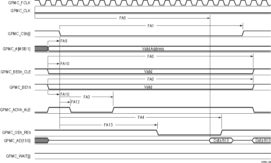
A. In GPMC_CSn[i], i is equal to 0, 1, 2 or
3. In GPMC_WAIT[j], j is equal to 0, 1, 2, or 3.
B. FA5 parameter illustrates amount of time
required to internally sample input data. It is expressed in number of GPMC functional
clock cycles. From start of read cycle and after FA5 functional clock cycles, input data
will be internally sampled by active functional clock edge. FA5 value must be stored
inside AccessTime register bits field.
C. GPMC_FCLK is an internal clock (GPMC
functional clock) not provided externally.
Figure 7-56 GPMC
and NOR Flash — Asynchronous Read — Single Word 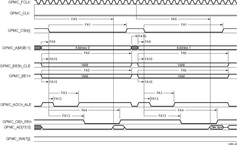
A. In GPMC_CSn[i], i is equal to 0, 1, 2 or
3. In GPMC_WAIT[j], j is equal to 0, 1, 2, or 3.
B. FA5 parameter illustrates amount of time
required to internally sample input data. It is expressed in number of GPMC functional
clock cycles. From start of read cycle and after FA5 functional clock cycles, input data
will be internally sampled by active functional clock edge. FA5 value must be stored
inside AccessTime register bits field.
C. GPMC_FCLK is an internal clock (GPMC
functional clock) not provided externally.
Figure 7-57 GPMC and NOR
Flash — Asynchronous Read — 32–Bit 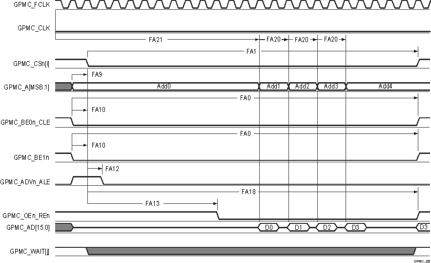
A. In GPMC_CSn[i], i is equal to 0, 1, 2 or
3. In GPMC_WAIT[j], j is equal to 0, 1, 2, or 3.
B. FA21 parameter illustrates amount of
time required to internally sample first input page data. It is expressed in number of
GPMC functional clock cycles. From start of read cycle and after FA21 functional clock
cycles, first input page data will be internally sampled by active functional clock edge.
FA21 calculation must be stored inside AccessTime register bits field.
C. FA20 parameter illustrates amount of
time required to internally sample successive input page data. It is expressed in number
of GPMC functional clock cycles. After each access to input page data, next input page
data will be internally sampled by active functional clock edge after FA20 functional
clock cycles. FA20 is also the duration of address phases for successive input page data
(excluding first input page data). FA20 value must be stored in PageBurstAccessTime
register bits field.
D. GPMC_FCLK is an internal clock (GPMC
functional clock) not provided externally.
Figure 7-58 GPMC and NOR
Flash — Asynchronous Read — Page Mode 4x16–Bit 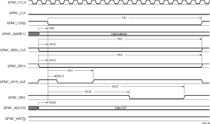
A. In GPMC_CSn[i], i is equal to 0, 1, 2 or
3. In GPMC_WAIT[j], j is equal to 0, 1, 2, or 3.
Figure 7-59 GPMC and NOR
Flash — Asynchronous Write — Single Word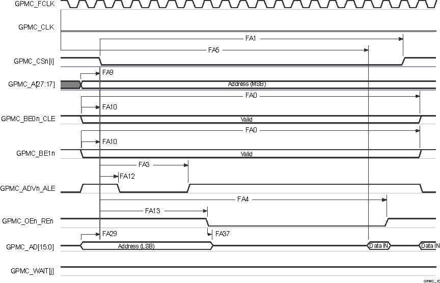
A. In GPMC_CSn[i], i is equal to 0, 1, 2 or
3. In GPMC_WAIT[j], j is equal to 0, 1, 2, or 3.
B. FA5 parameter illustrates amount of time
required to internally sample input data. It is expressed in number of GPMC functional
clock cycles. From start of read cycle and after FA5 functional clock cycles, input data
will be internally sampled by active functional clock edge. FA5 value must be stored
inside AccessTime register bits field.
C. GPMC_FCLK is an internal clock (GPMC
functional clock) not provided externally.
Figure 7-60 GPMC and
Multiplexed NOR Flash — Asynchronous Read — Single Word 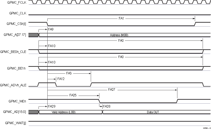
A. In GPMC_CSn[i], i is equal to 0, 1, 2 or
3. In GPMC_WAIT[j], j is equal to 0, 1, 2, or 3.
Figure 7-61 GPMC and
Multiplexed NOR Flash — Asynchronous Write — Single Word