ZHCSDF0C February 2015 – August 2015 TDC7200
PRODUCTION DATA.
- 1 特性
- 2 应用
- 3 说明
- 4 修订历史记录
- 5 Companion Device
- 6 Pin Configuration and Functions
- 7 Specifications
-
8 Detailed Description
- 8.1 Overview
- 8.2 Functional Block Diagram
- 8.3 Feature Description
- 8.4 Device Functional Modes
- 8.5 Programming
- 8.6
Register Maps
- 8.6.1 Register Initialization
- 8.6.2 CONFIG1: Configuration Register 1 R/W (address = 00h) [reset = 0h]
- 8.6.3 CONFIG2: Configuration Register 2 R/W (address = 01h) [reset = 40h]
- 8.6.4 INT_STATUS: Interrupt Status Register (address = 02h) [reset = 00h]
- 8.6.5 INT_MASK: Interrupt Mask Register R/W (address = 03h) [reset = 07h]
- 8.6.6 COARSE_CNTR_OVF_H: Coarse Counter Overflow High Value Register (address = 04h) [reset = FFh]
- 8.6.7 COARSE_CNTR_OVF_L: Coarse Counter Overflow Low Value Register (address = 05h) [reset = FFh ]
- 8.6.8 CLOCK_CNTR_OVF_H: Clock Counter Overflow High Register (address = 06h) [reset = FFh]
- 8.6.9 CLOCK_CNTR_OVF_L: Clock Counter Overflow Low Register (address = 07h) [reset = FFh]
- 8.6.10 CLOCK_CNTR_STOP_MASK_H: CLOCK Counter STOP Mask High Value Register (address = 08h) [reset = 00h]
- 8.6.11 CLOCK_CNTR_STOP_MASK_L: CLOCK Counter STOP Mask Low Value Register (address = 09h) [reset = 00h]
- 8.6.12 TIME1: Time 1 Register (address: 10h) [reset = 00_0000h]
- 8.6.13 CLOCK_COUNT1: Clock Count Register (address: 11h) [reset = 00_0000h]
- 8.6.14 TIME2: Time 2 Register (address: 12h) [reset = 00_0000h]
- 8.6.15 CLOCK_COUNT2: Clock Count Register (address: 13h) [reset = 00_0000h]
- 8.6.16 TIME3: Time 3 Register (address: 14h) [reset = 00_0000h]
- 8.6.17 CLOCK_COUNT3: Clock Count Registers (address: 15h) [reset = 00_0000h]
- 8.6.18 TIME4: Time 4 Register (address: 16h) [reset = 00_0000h]
- 8.6.19 CLOCK_COUNT4: Clock Count Register (address: 17h) [reset = 00_0000h]
- 8.6.20 TIME5: Time 5 Register (address: 18h) [reset = 00_0000h]
- 8.6.21 CLOCK_COUNT5: Clock Count Register (address: 19h) [reset = 00_0000h]
- 8.6.22 TIME6: Time 6 Register (address: 1Ah) [reset = 00_0000h]
- 8.6.23 CALIBRATION1: Calibration 1 Register (address: 1Bh ) [reset = 00_0000h]
- 8.6.24 CALIBRATION2: Calibration 2 Register (address: 1Ch ) [reset = 00_0000h]
- 9 Application and Implementation
- 10Power Supply Recommendations
- 11Layout
- 12器件和文档支持
- 13机械、封装和可订购信息
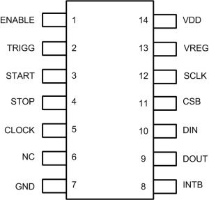
6 Pin Configuration and Functions
PW Package
14-Pin TSSOP
Top View

Pin Functions
| PIN | I/O | DESCRIPTION | |
|---|---|---|---|
| NAME | NO. | ||
| ENABLE | 1 | Input | Enable signal to TDC |
| TRIGG | 2 | Output | Trigger output signal |
| START | 3 | Input | START signal to TDC |
| STOP | 4 | Input | STOP signal to TDC |
| CLOCK | 5 | Input | Clock Input to TDC |
| N.C. | 6 | – | Not Connected |
| GND | 7 | Ground | Ground |
| INTB | 8 | Output | Interrupt to MCU, active low (open drain) |
| DOUT | 9 | Output | SPI Data Output |
| DIN | 10 | Input | SPI Data Input |
| CSB | 11 | Input | SPI Chip Select, active low |
| SCLK | 12 | Input | SPI clock |
| VREG | 13 | Output | LDO Output terminal for external decoupling cap |
| VDD | 14 | Power | Supply input |