ZHCSDF0C February 2015 – August 2015 TDC7200
PRODUCTION DATA.
- 1 特性
- 2 应用
- 3 说明
- 4 修订历史记录
- 5 Companion Device
- 6 Pin Configuration and Functions
- 7 Specifications
-
8 Detailed Description
- 8.1 Overview
- 8.2 Functional Block Diagram
- 8.3 Feature Description
- 8.4 Device Functional Modes
- 8.5 Programming
- 8.6
Register Maps
- 8.6.1 Register Initialization
- 8.6.2 CONFIG1: Configuration Register 1 R/W (address = 00h) [reset = 0h]
- 8.6.3 CONFIG2: Configuration Register 2 R/W (address = 01h) [reset = 40h]
- 8.6.4 INT_STATUS: Interrupt Status Register (address = 02h) [reset = 00h]
- 8.6.5 INT_MASK: Interrupt Mask Register R/W (address = 03h) [reset = 07h]
- 8.6.6 COARSE_CNTR_OVF_H: Coarse Counter Overflow High Value Register (address = 04h) [reset = FFh]
- 8.6.7 COARSE_CNTR_OVF_L: Coarse Counter Overflow Low Value Register (address = 05h) [reset = FFh ]
- 8.6.8 CLOCK_CNTR_OVF_H: Clock Counter Overflow High Register (address = 06h) [reset = FFh]
- 8.6.9 CLOCK_CNTR_OVF_L: Clock Counter Overflow Low Register (address = 07h) [reset = FFh]
- 8.6.10 CLOCK_CNTR_STOP_MASK_H: CLOCK Counter STOP Mask High Value Register (address = 08h) [reset = 00h]
- 8.6.11 CLOCK_CNTR_STOP_MASK_L: CLOCK Counter STOP Mask Low Value Register (address = 09h) [reset = 00h]
- 8.6.12 TIME1: Time 1 Register (address: 10h) [reset = 00_0000h]
- 8.6.13 CLOCK_COUNT1: Clock Count Register (address: 11h) [reset = 00_0000h]
- 8.6.14 TIME2: Time 2 Register (address: 12h) [reset = 00_0000h]
- 8.6.15 CLOCK_COUNT2: Clock Count Register (address: 13h) [reset = 00_0000h]
- 8.6.16 TIME3: Time 3 Register (address: 14h) [reset = 00_0000h]
- 8.6.17 CLOCK_COUNT3: Clock Count Registers (address: 15h) [reset = 00_0000h]
- 8.6.18 TIME4: Time 4 Register (address: 16h) [reset = 00_0000h]
- 8.6.19 CLOCK_COUNT4: Clock Count Register (address: 17h) [reset = 00_0000h]
- 8.6.20 TIME5: Time 5 Register (address: 18h) [reset = 00_0000h]
- 8.6.21 CLOCK_COUNT5: Clock Count Register (address: 19h) [reset = 00_0000h]
- 8.6.22 TIME6: Time 6 Register (address: 1Ah) [reset = 00_0000h]
- 8.6.23 CALIBRATION1: Calibration 1 Register (address: 1Bh ) [reset = 00_0000h]
- 8.6.24 CALIBRATION2: Calibration 2 Register (address: 1Ch ) [reset = 00_0000h]
- 9 Application and Implementation
- 10Power Supply Recommendations
- 11Layout
- 12器件和文档支持
- 13机械、封装和可订购信息
7 Specifications
7.1 Absolute Maximum Ratings
TA = 25°C , VDD = 3.3V, GND = 0V (unless otherwise noted).(1)(2)(3)| MIN | MAX | UNIT | |||
|---|---|---|---|---|---|
| VDD | Supply voltage | –0.3 | 3.9 | V | |
| VI | Terminal input voltage | –0.3 | VDD+0.3 | V | |
| VDIFF_IN | |Voltage differential| between any two input terminals | 3.9 | V | ||
| VIN_GND_VDD | |Voltage differential| between any input terminal and GND or VDD | 3.9 | V | ||
| II | Input current at any pin | –5 | 5 | mA | |
| TA | Ambient temperature | -40 | 125 | °C | |
| Tstg | Storage temperature | –65 | 150 | °C | |
(1) Stresses beyond those listed under Absolute Maximum Ratings may cause permanent damage to the device. These are stress ratings only, which do not imply functional operation of the device at these or any other conditions beyond those indicated under Recommended Operating Conditions. Exposure to absolute-maximum-rated conditions for extended periods may affect device reliability.
(2) The algebraic convention, whereby the most negative value is a minimum and the most positive value is a maximum
(3) All voltages are with respect to ground, unless otherwise specified.
7.2 ESD Ratings
| VALUE | UNIT | |||
|---|---|---|---|---|
| V(ESD) | Electrostatic discharge | Human-body model (HBM), per ANSI/ESDA/JEDEC JS-001(1) | ±1000 | V |
| Charged-device model (CDM), per JEDEC specification JESD22-C101(2) | ±250 | |||
(1) JEDEC document JEP155 states that 500-V HBM allows safe manufacturing with a standard ESD control process.
(2) JEDEC document JEP157 states that 250-V CDM allows safe manufacturing with a standard ESD control process.
7.3 Recommended Operating Conditions
TA = 25°C , VDD = 3.3V, GND = 0V (unless otherwise noted).| MIN | NOM | MAX | UNIT | ||
|---|---|---|---|---|---|
| VDD | Supply voltage | 2 | 3.6 | V | |
| VI | Terminal voltage | 0 | VDD | V | |
| VIH | Voltage input high | 0.7 × VDD | 3.6 | V | |
| VIL | Voltage input low | 0 | 0.3 × VDD | V | |
| FCALIB_CLK | Frequency (Reference/Calibration Clock) | 1 (1) | 8 | 16 | MHz |
| DUTYCLOCK | Input clock duty cycle | 50% | |||
| TIMING REQUIREMENTS: Measurement Mode 1 (1) | |||||
| T1STARTSTOP_Min | Minimum Time between Start and Stop Signal | 12 | ns | ||
| T1STOPSTOP_Min | Minimum Time between 2 Stop Signals | 67 | ns | ||
| T1STARTSTOP_Max | Maximum time bet. Start and Stop Signal | 500 | ns | ||
| T1STOPSTOP_Max | Maximum time bet. Start and last Stop Signal | 500 | ns | ||
| TIMING REQUIREMENTS: Measurement 2 (1) | |||||
| T2STARTSTOP_Min | Minimum Time between Start and Stop Signal | 2×tCLOCK | s | ||
| T2STOPSTOP_Min | Minimum Time between 2 Stop Signals | 2×tCLOCK | s | ||
| T2STARTSTOP_Max | Maximum time bet. Start and Stop Signal | (216-2)×tCLOCK | s | ||
| T2STOPSTOP_Max | Maximum. time bet. Start and last Stop Signal | (216-2)×tCLOCK | s | ||
| TIMING REQUIREMENTS: ENABLE INPUT | |||||
| TREN | Rise Time for Enable Signal (20%-80%) | 1 to 100 | ns | ||
| TFEN | Fall Time for Enable Signal (20%-80%) | 1 to 100 | ns | ||
| TIMING REQUIREMENTS: START, STOP, CLOCK | |||||
| TRST, TFST | Maximum rise, fall time for START, STOP signals (20%-80%) | 1 | ns | ||
| TRXCLK, TFXCLK | Maximum rise, fall time for external CLOCK (20%-80%) | 1 | ns | ||
| TIMING REQUIREMENTS: TRIGG | |||||
| TTRIGSTART | Time from TRIG to START | 5 | ns | ||
| TEMPERATURE | |||||
| TA | Ambient temperature | –40 | 85 | °C | |
| TJ | Junction temperature | –40 | 85 | °C | |
7.4 Thermal Information
| THERMAL METRIC(2) | TDC7200 | UNIT | |
|---|---|---|---|
| PW [TSSOP] | |||
| 14 PINS | |||
| RθJA | Junction-to-ambient thermal resistance | 134.9 | °C/W |
| RθJC(top) | Junction-to-case (top) thermal resistance | 63 | |
| RθJB | Junction-to-board thermal resistance | 76.8 | |
| ψJT | Junction-to-top characterization parameter | 12.4 | |
| ψJB | Junction-to-board characterization parameter | 76.2 | |
| θJA | Package thermal impedance | 113 | |
(1) Specified by design.
(2) For more information about traditional and new thermal metrics, see the IC Package Thermal Metrics application report, SPRA953.
7.5 Electrical Characteristics
TA = 25°C , VDD = 3.3 V, GND = 0 V (unless otherwise noted).| PARAMETER | TEST CONDITIONS | MIN | TYP | MAX | UNIT | ||
|---|---|---|---|---|---|---|---|
| TDC CHARACTERISTICS | |||||||
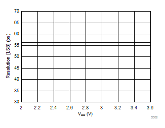
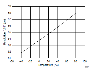
| LSB | Resolution | Single shot measurement | 55 | ps | |||
| TACC-2 | Accuracy (Mode 2) (1) | CLOCK = 8 MHz | 28 | ps | |||
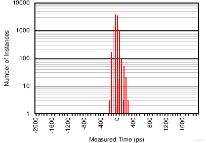
| TSTD-2 | Standard Deviation (Mode 2) | Measured time = 100 µs | 50 | ps | |||
| Measured time = 1 µs | 35 | ps | |||||
| OUTPUT CHARACTERISTICS: TRIGG, INTB, DOUT | |||||||
| VOH | Output voltage high | Isource = -2 mA | 2.31 | 2.95 | V | ||
| VOL | Output voltage low | Isink = 2 mA | 0.35 | 0.99 | V | ||
| INPUT CHARACTERISTICS: ENABLE, START, STOP, CLOCK, DIN, CSB,SCLK | |||||||
| Cin | Input capacitance (2) | 3 | pF | ||||
| POWER CONSUMPTION (see Measurement Mode 1 and Measurement Mode 2) | |||||||
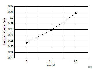
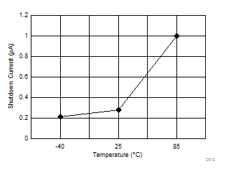
| Ish | Shutdown current | EN = LOW | 0.3 | 2 | µA | ||
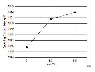
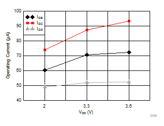
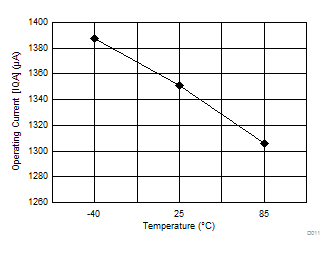
| IQA | Quiescent Current A | EN = HIGH; TDC running | 1.35 | mA | |||
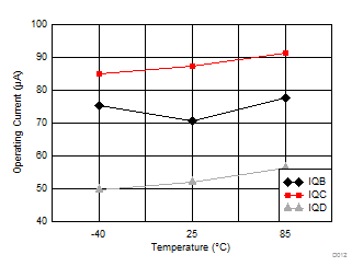
| IQB | Quiescent Current B | EN = HIGH; TDC OFF, Clock Counter running | 71 | µA | |||
| IQC | Quiescent Current C | EN = HIGH; measurement stopped, SPI communication only | 87 | µA | |||
| IQD | Quiescent Current D | TDC OFF, counter stopped, no communication | 50 | µA | |||
7.6 Timing Requirements
| MIN | NOM | MAX | UNIT | |||
|---|---|---|---|---|---|---|
| TIMING REQUIREMENTS: START, STOP INPUTS, CLOCK | ||||||
| PWSTART | Pulse width for Start Signal | 10 | ns | |||
| PWSTOP | Pulse width for Stop Signal | 10 | ns | |||
| SERIAL INTERFACE TIMING CHARACTERISTICS (VDD = 3.3 V, fSCLK = 20 MHz) (See Figure 1) | ||||||
| fSCLK | SCLK Frequency | 20 | MHz | |||
| t1 | SCLK period | 50 | ns | |||
| t2 | SCLK High Time | 16 | ns | |||
| t3 | SCLK Low Time | 16 | ns | |||
| t4 | DIN setup time | 4 | ns | |||
| t5 | DIN hold time | 4 | ns | |||
| t6 | CSB fall to SCLK rise | 6 | ns | |||
| t7 | Last SCLK rising edge to CSB rising edge | 6 | ns | |||
| t8 | Minimum pause time (CSB high) | 40 | ns | |||
| t9 | Clk fall to DOUT bus transition | 12 | ns | |||
(1) Accuracy is defined as the systematic error in the output signal; the error of the device excluding noise.
(2) Specified by design.
7.7 Switching Characteristics
TA = 25°C , VDD = 3.3 V, GND = 0 V (unless otherwise noted).| PARAMETER | TEST CONDITIONS | MIN | TYP | MAX | UNIT | |
|---|---|---|---|---|---|---|
| WAKE UP TIME | ||||||
| TWAKEUP_PERIOD | Time to be ready for Measurement | LSB within 0.3% of settled value | 300 | µs | ||
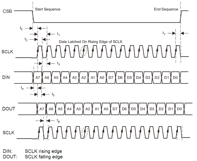 Figure 1. SPI Register Write: 8 bit Register Example
7.8 Typical Characteristics
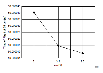
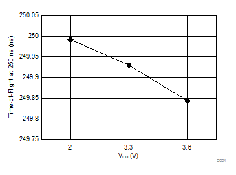
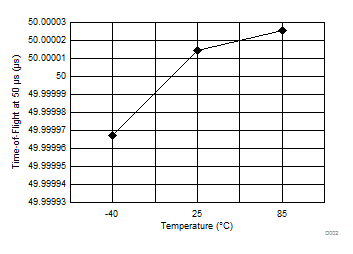
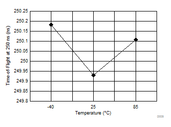
TA = 25°C , VDD = 3.3 V, GND = 0 V, CLOCK = 8 MHz, CALIBRATION2_PERIODS = 10, AVG_CYCLES = 1 Measurement, NUM_STOP = Single STOP, Measurement Mode 2 (unless otherwise noted).