ZHCSFY1F December 2016 – April 2024 TDP158
PRODUCTION DATA
- 1
- 1 特性
- 2 应用
- 3 说明
- 4 Pin Configuration and Functions
-
5 Specifications
- 5.1 Absolute Maximum Ratings
- 5.2 ESD Ratings
- 5.3 Recommended Operating Conditions
- 5.4 Thermal Information
- 5.5 Electrical Characteristics, Power Supply
- 5.6 Electrical Characteristics, Differential Input
- 5.7 Electrical Characteristics, TMDS Differential Output
- 5.8 Electrical Characteristics, DDC, I2C, HPD, and ARC
- 5.9 Electrical Characteristics, TMDS Differential Output in DP-Mode
- 5.10 Switching Characteristics, TMDS
- 5.11 Switching Characteristics, HPD
- 5.12 Switching Characteristics, DDC and I2C
- 5.13 Typical Characteristics
- 6 Parameter Measurement Information
-
7 Detailed Description
- 7.1 Overview
- 7.2 Functional Block Diagram
- 7.3 Feature Description
- 7.4 Device Functional Modes
- 7.5
Register Maps
- 7.5.1 Local I2C Control BIT Access TAG Convention
- 7.5.2 BIT Access Tag Conventions
- 7.5.3 CSR Bit Field Definitions, DEVICE_ID (address = 00h≅07h)
- 7.5.4 CSR Bit Field Definitions, REV_ID (address = 08h )
- 7.5.5 CSR Bit Field Definitions – MISC CONTROL 09h (address = 09h)
- 7.5.6 CSR Bit Field Definitions – MISC CONTROL 0Ah (address = 0Ah)
- 7.5.7 CSR Bit Field Definitions – MISC CONTROL 0Bh (address = 0Bh)
- 7.5.8 CSR Bit Field Definitions – MISC CONTROL 0Ch (address = 0Ch)
- 7.5.9 CSR Bit Field Definitions, Equalization Control Register (address = 0Dh)
- 7.5.10 CSR Bit Field Definitions, POWER MODE STATUS (address = 20h)
- 7.5.11 CSR Bit Field Definitions, DP-Mode and INDIVIDUAL LANE CONTROL (address = 30h)
- 7.5.12 CSR Bit Field Definitions, DP-Mode and INDIVIDUAL LANE CONTROL (address = 31h)
- 7.5.13 CSR Bit Field Definitions, DP-Mode and INDIVIDUAL LANE CONTROL (address = 32h)
- 7.5.14 CSR Bit Field Definitions, DP-Mode and INDIVIDUAL LANE CONTROL (address = 33h)
- 7.5.15 CSR Bit Field Definitions, DP-Mode and INDIVIDUAL LANE CONTROL (address = 34h)
- 7.5.16 CSR Bit Field Definitions, DP-Mode and INDIVIDUAL LANE CONTROL (address = 35h)
- 7.5.17 CSR Bit Field Definitions, DP-Mode and INDIVIDUAL LANE CONTROL (address = 4Dh)
- 7.5.18 CSR Bit Field Definitions, DP-Mode and INDIVIDUAL LANE CONTROL (address = 4Eh)
- 7.5.19 CSR Bit Field Definitions, DP-Mode and INDIVIDUAL LANE CONTROL (address = 4Fh)
- 8 Application and Implementation
- 9 Device and Documentation Support
- 10Revision History
- 11Mechanical, Packaging, and Orderable Information
7.3.11 Pre-Emphasis
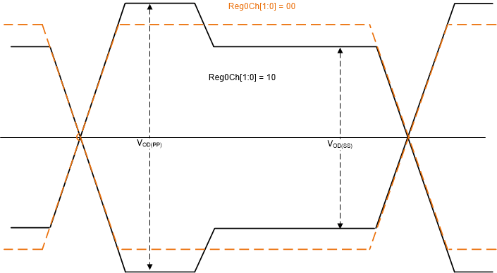
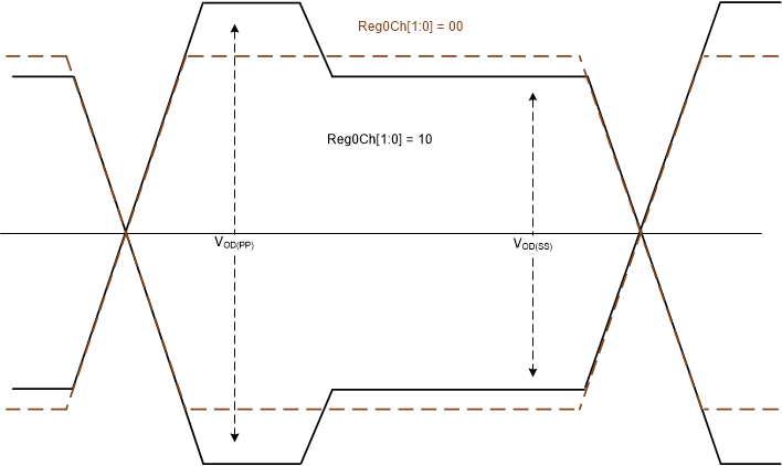
The TDP158 provides pre-emphasis on the data lanes allowing the output signal pre-conditioning to offset interconnect losses between the TDP158 outputs and a TMDS receiver. Pre-emphasis is not implemented on the clock lane unless the TDP158 is in DP mode; at which time, it becomes a data lane. The default value for pre-emphasis is 0dB. There are two methods to implement pre-emphasis, pin strapping or through I2C programming. When using pin strapping, the SDA_CTL/PRE pin controls global pre-emphasis values of 0dB or 3.5dB. Through I2C, reg0Ch[1:0] pre-emphasis values are 0dB, 3.5dB, and 6dB. The 6dB value has different meanings when the device is in normal operational mode (reg09h[5] = 0) or when the TDP158 has been put into DP-mode (reg09h[5] = 1). As Figure 7-6 shows, the 6dB pre-emphasis setting will result in an output of 3dB of pre-emphasis with 3dB of de-emphasis when device is in normal HDMI operation. As Figure 7-7 shows, the output will be about 5dB pre-emphasis with a 1dB de-emphasis when selecting 6dB pre-emphasis setting for DP-mode. VOD(PP) value will not go above 1V.
 Figure 7-6 6dB Pre-Emphasis Setting in Normal
Operation
 Figure 7-7 6dB Pre-Emphasis in DP-Mode
| Global Control | Independent Lane Control | |||||
|---|---|---|---|---|---|---|
| Mode | Reg09h[6] Lane CTL | Reg09[5] Mode CTL | P0_Reg0C[7:0] | Reg09h[6] Lane CTL | Reg09[5] Mode CTL | P0_Reg0C[7:0] |
| HDMI | 0 | 0 | 8’h00 | 1 | 0 | 8’h00 |
| DP SWG0, PRE0 | 0 | 1 | 8’h80 | 1 | 1 | 8’h80 |
| DP SWG0, PRE1 | 0 | 1 | 8’hC1 | 1 | 1 | 8’hC1 |
| DP SWG0, PRE2 | 0 | 1 | 8’h42 | 1 | 1 | 8’h42 |
| DP SWG1, PRE0 | 0 | 1 | 8’hC0 | 1 | 1 | 8’hA0 |
| DP SWG1, PRE1 | 0 | 1 | 8’hF1 | 1 | 1 | 8’h21 |
| DP SWG1, PRE2 | 0 | 1 | 8’h52 | 1 | 1 | 8’h62 |
| DP SWG2, PRE0 | 0 | 1 | 8’h20 | 1 | 1 | 8’h00 |
| DP SWG2, PRE1 | 0 | 1 | 8’h51 | 1 | 1 | 8’h61 |