ZHCSFY1F December 2016 – April 2024 TDP158
PRODUCTION DATA
- 1
- 1 特性
- 2 应用
- 3 说明
- 4 Pin Configuration and Functions
-
5 Specifications
- 5.1 Absolute Maximum Ratings
- 5.2 ESD Ratings
- 5.3 Recommended Operating Conditions
- 5.4 Thermal Information
- 5.5 Electrical Characteristics, Power Supply
- 5.6 Electrical Characteristics, Differential Input
- 5.7 Electrical Characteristics, TMDS Differential Output
- 5.8 Electrical Characteristics, DDC, I2C, HPD, and ARC
- 5.9 Electrical Characteristics, TMDS Differential Output in DP-Mode
- 5.10 Switching Characteristics, TMDS
- 5.11 Switching Characteristics, HPD
- 5.12 Switching Characteristics, DDC and I2C
- 5.13 Typical Characteristics
- 6 Parameter Measurement Information
-
7 Detailed Description
- 7.1 Overview
- 7.2 Functional Block Diagram
- 7.3 Feature Description
- 7.4 Device Functional Modes
- 7.5
Register Maps
- 7.5.1 Local I2C Control BIT Access TAG Convention
- 7.5.2 BIT Access Tag Conventions
- 7.5.3 CSR Bit Field Definitions, DEVICE_ID (address = 00h≅07h)
- 7.5.4 CSR Bit Field Definitions, REV_ID (address = 08h )
- 7.5.5 CSR Bit Field Definitions – MISC CONTROL 09h (address = 09h)
- 7.5.6 CSR Bit Field Definitions – MISC CONTROL 0Ah (address = 0Ah)
- 7.5.7 CSR Bit Field Definitions – MISC CONTROL 0Bh (address = 0Bh)
- 7.5.8 CSR Bit Field Definitions – MISC CONTROL 0Ch (address = 0Ch)
- 7.5.9 CSR Bit Field Definitions, Equalization Control Register (address = 0Dh)
- 7.5.10 CSR Bit Field Definitions, POWER MODE STATUS (address = 20h)
- 7.5.11 CSR Bit Field Definitions, DP-Mode and INDIVIDUAL LANE CONTROL (address = 30h)
- 7.5.12 CSR Bit Field Definitions, DP-Mode and INDIVIDUAL LANE CONTROL (address = 31h)
- 7.5.13 CSR Bit Field Definitions, DP-Mode and INDIVIDUAL LANE CONTROL (address = 32h)
- 7.5.14 CSR Bit Field Definitions, DP-Mode and INDIVIDUAL LANE CONTROL (address = 33h)
- 7.5.15 CSR Bit Field Definitions, DP-Mode and INDIVIDUAL LANE CONTROL (address = 34h)
- 7.5.16 CSR Bit Field Definitions, DP-Mode and INDIVIDUAL LANE CONTROL (address = 35h)
- 7.5.17 CSR Bit Field Definitions, DP-Mode and INDIVIDUAL LANE CONTROL (address = 4Dh)
- 7.5.18 CSR Bit Field Definitions, DP-Mode and INDIVIDUAL LANE CONTROL (address = 4Eh)
- 7.5.19 CSR Bit Field Definitions, DP-Mode and INDIVIDUAL LANE CONTROL (address = 4Fh)
- 8 Application and Implementation
- 9 Device and Documentation Support
- 10Revision History
- 11Mechanical, Packaging, and Orderable Information
8.4.1 Layout Guidelines
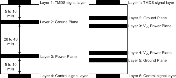
For the TDP158 on a high-K board, it is required to solder the PowerPAD™ onto the thermal land to ground. A thermal land is the area of solder-tinned-copper underneath the PowerPAD™ package. On a high-K board the TDP158 can operate over the full temperature range by soldering the PowerPAD™ onto the thermal land. On a low-K board, for the device to operate across the temperature range on a low-K board, a 1-oz Cu trace connecting the GND pins to the thermal land must be used. A simulation shows RθJA = 100.84°C/W allowing 545mW power dissipation at 70°C ambient temperature. A general PCB design guide for PowerPAD packages is provided in the document SLMA002. TI recommends using a four layer stack up at a minimum to accomplish a low-EMI PCB design. TI recommends six layers as the TDP158 is a two voltage rail device.
- Routing the high-speed TMDS traces on the top layer avoids the use of vias, avoids the introduction of their inductances, and allows for clean interconnects from the HDMI connectors to the Redriver inputs and outputs. It is important to match the electrical length of these high speed traces to minimize both inter-pair and intra-pair skew.
- Placing a solid ground plane next to the high-speed single layer establishes controlled impedance for transmission link interconnects and provides an excellent low –inductance path for the return current flow.
- Placing a power plane next to the ground plane creates and additional high-frequency bypass capacitance.
- Routing slower seed control signals on the bottom layer allows for greater flexibility as these signal links usually have margin to tolerate discontinuities such as vias.
- If an additional supply voltage plane or signal layer is needed, add a second power/ground plane system to the stack to keep symmetry. This makes the stack mechanically stable and prevents it from warping. Also the power and ground plane of each power system can be place closer together, thus increasing the high frequency bypass capacitance significantly.
 Figure 8-7 Recommended 4 – or 6 – Layer PCB Stack