ZHCSQ95H March   2000  – March 2022 TFP401 , TFP401A

PRODUCTION DATA  

  1. 特性
  2. 应用
  3. 说明
  4. Revision History
  5. 说明(续)
  6. Pin Configuration and Functions
  7. Specifications
    1. 7.1 Absolute Maximum Ratings (1)
    2. 7.2 ESD Ratings
    3. 7.3 Recommended Operating Conditions
    4. 7.4 Thermal Information
    5. 7.5 DC Digital I/O Electrical Characteristics
    6. 7.6 DC Electrical Characteristics
    7. 7.7 AC Electrical Characteristics
    8. 7.8 Typical Characteristics
  8. Parameter Measurement Information
  9. Detailed Description
    1. 9.1 Overview
    2. 9.2 Functional Block Diagram
    3. 9.3 Feature Description
      1. 9.3.1 TMDS Pixel Data and Control Signal Encoding
      2. 9.3.2 TFP401/401A Clocking and Data Synchronization
      3. 9.3.3 TFP401/401A TMDS Input Levels and Input Impedance Matching
      4. 9.3.4 TFP401A Incorporates HSYNC Jitter Immunity
    4. 9.4 Device Functional Modes
      1. 9.4.1 TFP401/401A Modes of Operation
      2. 9.4.2 TFP401/401A Output Driver Configurations
        1. 9.4.2.1 Output Driver Power Down
        2. 9.4.2.2 Drive Strength
        3. 9.4.2.3 Time-Staggered Pixel Output
        4. 9.4.2.4 Power Management
        5. 9.4.2.5 Sync Detect
  10. 10Applications and Implementation
    1. 10.1 Application Information
    2. 10.2 Typical Application
      1. 10.2.1 Design Requirements
      2. 10.2.2 Detailed Design Procedure
        1. 10.2.2.1 Data and Control Signals
        2. 10.2.2.2 Configuration Options
        3. 10.2.2.3 Power Supplies Decoupling
      3. 10.2.3 Application Curve
  11. 11Power Supply Recommendations
  12. 12Layout
    1. 12.1 Layout Guidelines
      1. 12.1.1 Layer Stack
      2. 12.1.2 Routing High-Speed Differential Signal Traces (RxC–, RxC+, Rx0–, Rx0+, Rx1–, Rx1+, Rx2–, Rx2+)
      3. 12.1.3 DVI Connector
    2. 12.2 Layout Example
    3. 12.3 TI PowerPAD 100-TQFP Package
  13. 13Device and Documentation Support
    1. 13.1 接收文档更新通知
    2. 13.2 支持资源
    3. 13.3 Trademarks
    4. 13.4 Electrostatic Discharge Caution
    5. 13.5 术语表
  14. 14Mechanical, Packaging, and Orderable Information

封装选项

机械数据 (封装 | 引脚)
散热焊盘机械数据 (封装 | 引脚)
订购信息

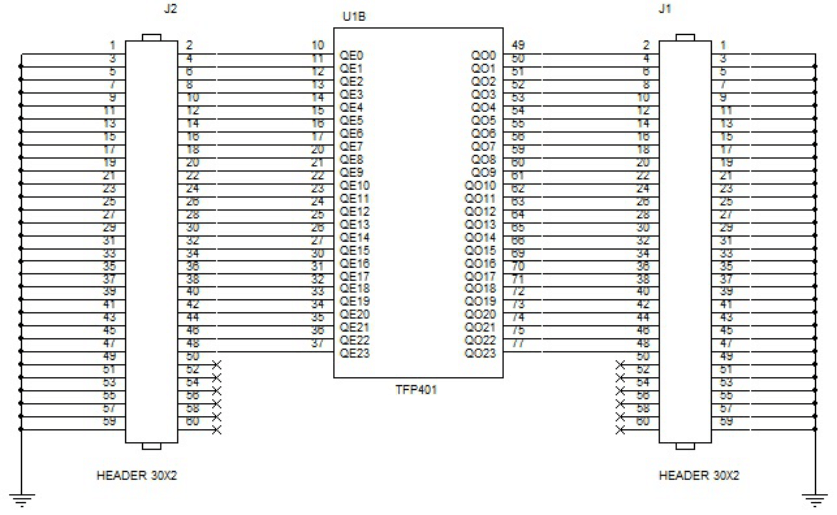
Data and Control Signals

The trace length of data and control signals out of the receiver should be kept as close to equal as possible. Trace separation should be ≈5X Height. As a general rule, traces also should be less than 2.8 inches if possible (longer traces can be acceptable).

Equation 1. Delay = 85 × SQRT ER

where

  • ER = 4.35
  • Relative permittivity of 50% resin FR-4 at 1 GHz
  • Delay = 177 pS/inch
Equation 2. Length of rising edge = TR (picoseconds) ÷ Delay

where

  • TR = 3 nS
  • = 3000 ps ÷ 177 ps per inch
  • = 16.9 inches
Equation 3. Length of rising edge ÷ 6 = Maximum length of trace for lumped circuit

where

  • 16.9 ÷ 6 = 2.8 inches
GUID-0BC300AA-9E54-4F52-AC99-D7F76B9EB45F-low.gifFigure 10-2 Data and Control Signals Design