ZHCSAH8B November 2012 – March 2022 TFP401A-Q1
PRODUCTION DATA
- 1 特性
- 2 应用
- 3 说明
- 4 Revision History
- 5 Pin Configuration and Functions
-
6 Specifications
- 6.1 Absolute Maximum Ratings
- 6.2 ESD Ratings
- 6.3 Recommended Operating Conditions
- 6.4 Thermal Information
- 6.5 DC Digital I/O Electrical Characteristics
- 6.6 DC Electrical Characteristics
- 6.7 AC Electrical Characteristics
- 6.8 Timing Requirements
- 6.9 Switching Characteristics
- 6.10 Typical Characteristics
- 7 Detailed Description
- 8 Application and Implementation
- 9 Device and Documentation Support
- 10Mechanical, Packaging, and Orderable Information
封装选项
机械数据 (封装 | 引脚)
- PZP|100
散热焊盘机械数据 (封装 | 引脚)
- PZP|100
订购信息
8.1.1.2.1 Data and Control Signals
The trace length of data and control signals out of the receiver should be kept as close to equal as possible. Trace separation should be ≈5X Height. As a general rule, traces also should be less than 2.8 inches if possible (longer traces can be acceptable).
Calculation:
Equation 1. Delay = 85 × SQRT er
Equation 2. er = 4.35; relative permitivity of 50% resin FR-4 at 1 GHz
Equation 3. Delay = 177 pS/inch
Equation 4. Length of rising edge = Tr(picoseconds)/Delay; Tr = 3 nS
Equation 5. = 3000 ps/177 ps per inch
Equation 6. = 16.9 inches
Equation 7. Length of rising edge / 6 = Maximum length of
trace for lumped circuit
Equation 8. 16.9 / 6 = 2.8 inches
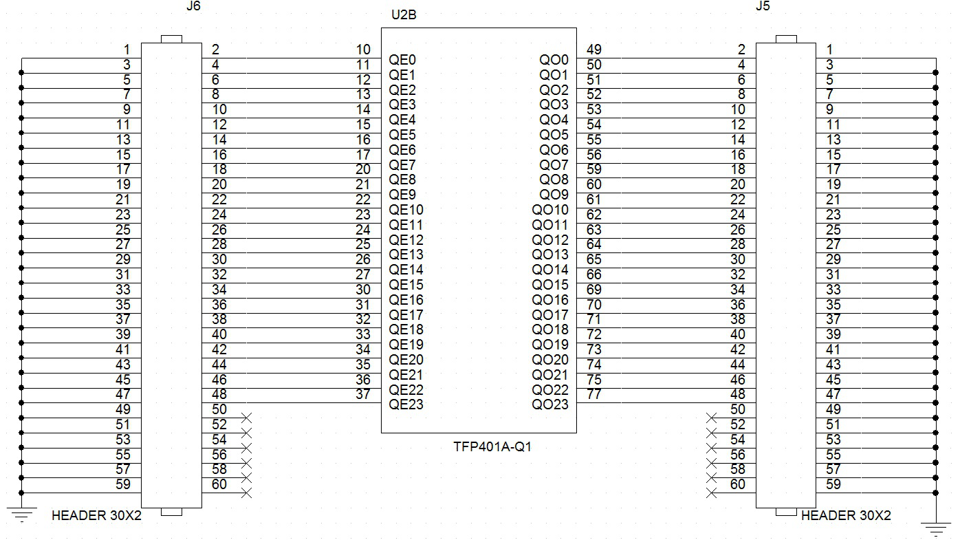
 Figure 8-2 TFP401A-Q1 App Info Data and Control Signals