ZHCSAH8B November 2012 – March 2022 TFP401A-Q1
PRODUCTION DATA
- 1 特性
- 2 应用
- 3 说明
- 4 Revision History
- 5 Pin Configuration and Functions
-
6 Specifications
- 6.1 Absolute Maximum Ratings
- 6.2 ESD Ratings
- 6.3 Recommended Operating Conditions
- 6.4 Thermal Information
- 6.5 DC Digital I/O Electrical Characteristics
- 6.6 DC Electrical Characteristics
- 6.7 AC Electrical Characteristics
- 6.8 Timing Requirements
- 6.9 Switching Characteristics
- 6.10 Typical Characteristics
- 7 Detailed Description
- 8 Application and Implementation
- 9 Device and Documentation Support
- 10Mechanical, Packaging, and Orderable Information
封装选项
机械数据 (封装 | 引脚)
- PZP|100
散热焊盘机械数据 (封装 | 引脚)
- PZP|100
订购信息
8.3.1.1 Layer Stack
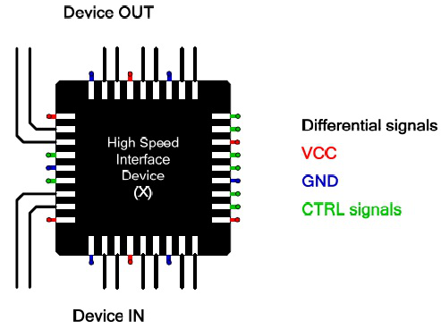
The pinout of Texas Instruments High Speed Interface (HSI) devices features differential signal pairs and the remaining signals comprise the supply rails, VCC and ground, and lower speed signals such as control pins. As an example, consider a device X which is a repeater/re-driver, so both its inputs and outputs are high-speed differential signals. These guidelines can be applied to other high-speed devices such as drivers, receivers, multiplexers, and so on.
A minimum of four layers is required to accomplish a low EMI PCB design. Layer stacking should be in the following order (top-to-bottom): high-speed differential signal layer, ground plane, power plane and control signal layer.
 Figure 8-7 Layer Stack