ZHCSAH8B November 2012 – March 2022 TFP401A-Q1
PRODUCTION DATA
- 1 特性
- 2 应用
- 3 说明
- 4 Revision History
- 5 Pin Configuration and Functions
-
6 Specifications
- 6.1 Absolute Maximum Ratings
- 6.2 ESD Ratings
- 6.3 Recommended Operating Conditions
- 6.4 Thermal Information
- 6.5 DC Digital I/O Electrical Characteristics
- 6.6 DC Electrical Characteristics
- 6.7 AC Electrical Characteristics
- 6.8 Timing Requirements
- 6.9 Switching Characteristics
- 6.10 Typical Characteristics
- 7 Detailed Description
- 8 Application and Implementation
- 9 Device and Documentation Support
- 10Mechanical, Packaging, and Orderable Information
封装选项
机械数据 (封装 | 引脚)
- PZP|100
散热焊盘机械数据 (封装 | 引脚)
- PZP|100
订购信息
7.3.3 TFP401A-Q1 TMDS Input Levels and Input Impedance Matching
The TMDS inputs to the TFP401A-Q1 receiver have a fixed single-ended termination to AVDD. A laser trim process internally optimizes the TFP401A-Q1 device to fix the impedance precisely at 50 Ω. The device functions normally with or without a resistor on the EXT_RES pin, so it remains drop-in compatible with current sockets. The fixed impedance eliminates the need for an external resistor while providing optimum impedance matching to standard 50-Ω DVI cables.
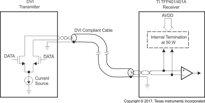
Figure 7-1 shows a conceptual schematic of a DVI transmitter and TFP401A-Q1 receiver connection. A transmitter drives the twisted-pair cable through a current source, usually using an open-drain type of output driver. The internal resistor, matched to the cable impedance at the TFP401A-Q1 input, provides a pullup to AVDD. Naturally, with the transmitter disconnected and the TFP401A-Q1 DVI inputs left unconnected, the TFP401A-Q1 receiver inputs pull up to AVDD. Figure 7-2 shows the single-ended differential signal and full-differential signal. The design of the TFP401A-Q1 device is for response to differential signal swings ranging from 150 mV to 1.56 V, with common-mode voltages ranging from (AVDD – 300 mV) to (AVDD – 37 mV).
 Figure 7-1 TMDS Differential Input and Transmitter Connection
 Figure 7-2 TMDS Inputs