ZHCSAH8B November 2012 – March 2022 TFP401A-Q1
PRODUCTION DATA
- 1 特性
- 2 应用
- 3 说明
- 4 Revision History
- 5 Pin Configuration and Functions
-
6 Specifications
- 6.1 Absolute Maximum Ratings
- 6.2 ESD Ratings
- 6.3 Recommended Operating Conditions
- 6.4 Thermal Information
- 6.5 DC Digital I/O Electrical Characteristics
- 6.6 DC Electrical Characteristics
- 6.7 AC Electrical Characteristics
- 6.8 Timing Requirements
- 6.9 Switching Characteristics
- 6.10 Typical Characteristics
- 7 Detailed Description
- 8 Application and Implementation
- 9 Device and Documentation Support
- 10Mechanical, Packaging, and Orderable Information
封装选项
机械数据 (封装 | 引脚)
- PZP|100
散热焊盘机械数据 (封装 | 引脚)
- PZP|100
订购信息
7.3.4 TFP401A-Q1 Device Incorporates HSYNC Jitter Immunity
Several DVI transmitters available in the market introduce jitter on the transmitted HSYNC and VSYNC signals during the TMDS encryption process. The HSYNC signal can shift by one pixel position (one clock) from nominal in either direction, resulting in up to two cycles of HSYNC shift. This jitter carries through to the DVI receiver, and if the position of HSYNC shifts continuously, the receiver can lose track of the input timing, causing pixel noise to occur on the display. For this reason, one should use a DVI-compliant receiver with HSYNC jitter immunity in all displays that could be connected to host PCs with transmitters that have this HSYNC jitter problem.
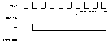
The TFP401A-Q1 integrates HSYNC regeneration circuitry that provides a seamless interface to these noncompliant transmitters. The regeneration circuitry always fixes the position of the data enable (DE) signal in relation to data, irrespective of the location of HSYNC. The TFP401A-Q1 receiver uses the DE and clock signals to recreate stable vertical and horizontal sync signals. The circuit filters the HSYNC output of the receiver and shifts HSYNC to the nearest eighth bit boundary, producing a stable output with respect to the data, as shown in Figure 7-3. This ensures accurate data synchronization at the input of the display timing controller.
This HSYNC regeneration circuit is transparent to the monitor, and removal is unnecessary even if the transmitted HSYNC is stable. For example, the PanelBus line of DVI 1.0-compliant transmitters, such as the TFP6422 and TFP420, do not have the HSYNC jitter problem. The TFP401A-Q1 device operates correctly with either compliant or noncompliant transmitters. In contrast, the TFP401A-Q1 device is ideal for customers who have control over the transmit portion of the design, such as bundled-system manufacturers and for internal monitor use (the DVI connection between monitor and panel modules).
 Figure 7-3 HSYNC Regeneration Timing Diagram