ZHCSQB3A january   2023  – july 2023 THS2630

PRODUCTION DATA  

  1.   1
  2. 特性
  3. 应用
  4. 说明
  5. Revision History
  6. Pin Configuration and Functions
  7. Specifications
    1. 6.1 Absolute Maximum Ratings
    2. 6.2 ESD Ratings
    3. 6.3 Recommended Operating Conditions
    4. 6.4 Thermal Information
    5. 6.5 Electrical Characteristics
    6. 6.6 Typical Characteristics
  8. Detailed Description
    1. 7.1 Overview
    2. 7.2 Functional Block Diagram
    3. 7.3 Feature Description
    4. 7.4 Device Functional Modes
      1. 7.4.1 Power-Down Mode
  9. Application and Implementation
    1. 8.1 Application Information
      1. 8.1.1 Output Common-Mode Voltage
        1. 8.1.1.1 Resistor Matching
      2. 8.1.2 Driving a Capacitive Load
      3. 8.1.3 Data Converters
      4. 8.1.4 Single-Supply Applications
    2. 8.2 Typical Application
      1. 8.2.1 Design Requirements
      2. 8.2.2 Detailed Design Procedure
        1. 8.2.2.1 Active Antialias Filtering
      3. 8.2.3 Application Curve
    3. 8.3 Power Supply Recommendations
    4. 8.4 Layout
      1. 8.4.1 Layout Guidelines
        1. 8.4.1.1 PowerPAD™ Integrated Circuit Package Design Considerations
      2. 8.4.2 Layout Example
  10. Device and Documentation Support
    1. 9.1 Documentation Support
      1. 9.1.1 Related Documentation
    2. 9.2 接收文档更新通知
    3. 9.3 支持资源
    4. 9.4 Trademarks
    5. 9.5 静电放电警告
    6. 9.6 术语表
  11. 10Mechanical, Packaging, and Orderable Information

封装选项

机械数据 (封装 | 引脚)
散热焊盘机械数据 (封装 | 引脚)
订购信息

Typical Application

For signal conditioning in ADC applications, it is important to limit the input frequency to the ADC. Low-pass filters can prevent the aliasing of the high-frequency noise with the frequency of operation. Figure 8-5 shows a method by which the noise may be filtered in the THS2630.

Figure 8-5 shows a typical application design example for the THS2630 device in active low-pass filter topology driving and ADC.
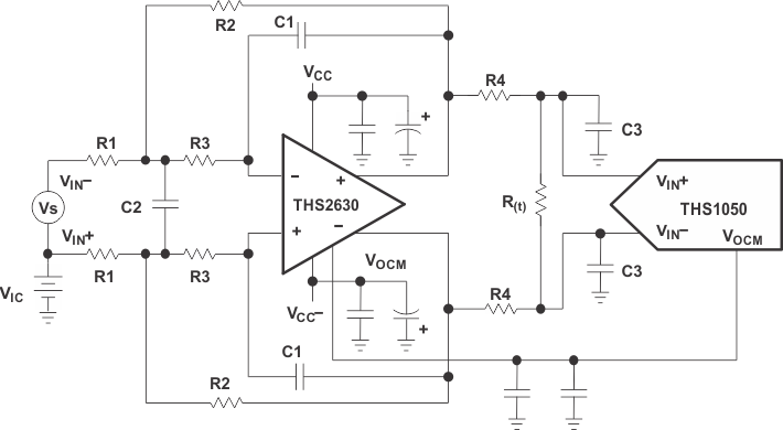
GUID-C660F0D3-BEB3-40D4-BF8E-DF2C5D0E1A30-low.gifFigure 8-5 Antialias Filtering