SLOS382E September 2001 – May 2015 THS3122 , THS3125
PRODUCTION DATA.
- 1 Features
- 2 Applications
- 3 Description
- 4 Revision History
- 5 Device Options
- 6 Pin Configuration and Functions
-
7 Specifications
- 7.1 Absolute Maximum Ratings
- 7.2 Dissipation Ratings Table
- 7.3 Recommended Operating Conditions
- 7.4 Electrical Characteristics: Dynamic Performance
- 7.5 Electrical Characteristics: Noise and Distortion Performance
- 7.6 Electrical Characteristics: DC Performance
- 7.7 Electrical Characteristics: Input Characteristics
- 7.8 Electrical Characteristics: Output Characteristics
- 7.9 Electrical Characteristics: Power Supply
- 7.10 Electrical Characteristics: Shutdown Characteristics (THS3125 Only)
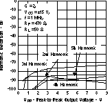
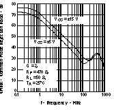
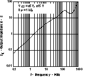
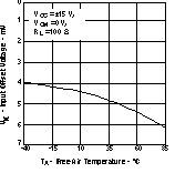
- 7.11 Typical Characteristics: Table Of Graphs
- 7.12 Typical Characteristics
- 8 Detailed Description
- 9 Application and Implementation
- 10Layout
- 11Device and Documentation Support
- 12Mechanical, Packaging, and Orderable Information
封装选项
机械数据 (封装 | 引脚)
散热焊盘机械数据 (封装 | 引脚)
- DDA|8
订购信息
7 Specifications
7.1 Absolute Maximum Ratings
over operating free-air temperature range (unless otherwise noted)(1)| MIN | MAX | UNIT | ||
|---|---|---|---|---|
| Supply voltage, VCC+ to VCC– | 33 | V | ||
| Input voltage | –VCC | +VCC | V | |
| Differential input voltage | –4 | +4 | V | |
| Output current(2) | 550 | mA | ||
| Total power dissipation at (or below) +25°C free-air temperature | See Dissipation Ratings Table | |||
| Maximum junction temperature | 150 | °C | ||
| Operating free-air temperature, TA | Commercial | 0 | 70 | °C |
| Industrial | –40 | +85 | °C | |
| Storage temperature, Tstg | Commercial | –65 | +125 | °C |
| Industrial | –65 | +125 | °C | |
(1) Stresses beyond those listed under Absolute Maximum Ratings may cause permanent damage to the device. These are stress ratings only, which do not imply functional operation of the device at these or any other conditions beyond those indicated under Recommended Operating Conditions. Exposure to absolute-maximum-rated conditions for extended periods may affect device reliability.
(2) The THS3122 and THS3125 may incorporate a PowerPAD on the underside of the chip. This pad acts as a heatsink and must be connected to a thermally dissipating plane for proper power dissipation. Failure to do so may result in exceeding the maximum junction temperature which could permanently damage the device. See TI Technical Brief SLMA002 for more information about utilizing the PowerPAD thermally-enhanced package.
7.2 Dissipation Ratings Table
| PACKAGE | θJA | TA = +25°C POWER RATING |
|---|---|---|
| D-8 | 95°C/W(1) | 1.32 W |
| DDA | 67°C/W | 1.87 W |
| D-14 | 66.6°C/W(1) | 1.88 W |
| PWP | 37.5°C/W | 3.3 W |
(1) These data were taken using the JEDEC proposed high-K test PCB. For the JEDEC low-K test PCB, the θJA is 168°C/W for the D-8 package and 122.3°C/W for the D-14 package.
7.3 Recommended Operating Conditions
| MIN | NOM | MAX | UNIT | ||
|---|---|---|---|---|---|
| Supply voltage, VCC+ to VCC– | Dual supply | ±5 | ±15 | V | |
| Single supply | 10 | 30 | V | ||
| Operating free-air temperature, TA | C-suffix | 0 | +70 | °C | |
| I-suffix | –40 | +85 | °C | ||
7.4 Electrical Characteristics: Dynamic Performance
Over operating free-air temperature range, TA = +25°C, VCC = ±15 V, RF = 750 Ω, and RL = 100 Ω (unless otherwise noted).| PARAMETER | TEST CONDITIONS | MIN | TYP | MAX | UNIT | ||||
|---|---|---|---|---|---|---|---|---|---|
| BW | Small-signal bandwidth (–3 dB) | RL = 50 Ω | RF = 50 Ω, G = 1 | VCC = ±5 V | 138 | MHz | |||
| VCC = ±15 V | 160 | MHz | |||||||
| RL = 50 Ω | RF = 470 Ω, G = 2 | VCC = ±5 V | 126 | MHz | |||||
| VCC = ±15 V | 128 | MHz | |||||||
| Bandwidth (0.1 dB) | RF = 470 Ω, G = 2 | VCC = ±5 V | 20 | MHz | |||||
| VCC = ±15 V | 30 | MHz | |||||||
| Full power bandwidth | G = –1 | VO(PP) = 4 V | VCC = ±5 V | 47 | MHz | ||||
| VO(PP) = 20 V | VCC = ±15 V | 64 | MHz | ||||||
| SR | Slew rate(1), G = 8 | G = 2, RF = 680Ω | VO = 10 VPP | VCC = ±15 V | 1550 | V/µs | |||
| VO = 5 VPP | VCC = ±5 V | 500 | V/µs | ||||||
| VCC = ±15 V | 1000 | V/µs | |||||||
| ts | Settling time to 0.1% | G = –1 | VO = 2 VPP | VCC = ±5 V | 53 | ns | |||
| VO= 5 VPP | VCC = ±15 V | 64 | ns | ||||||
(1) Slew rate is defined from the 25% to the 75% output levels.
7.5 Electrical Characteristics: Noise and Distortion Performance
Over operating free-air temperature range, TA = +25°C, VCC = ±15 V, RF = 750 Ω, and RL = 100 Ω (unless otherwise noted).| PARAMETER | TEST CONDITIONS | MIN | TYP | MAX | UNIT | |||
|---|---|---|---|---|---|---|---|---|
| THD | Total harmonic distortion | G = 2, RF = 470 Ω, VCC= ±15 V, f = 1 MHz |
VO(PP) = 2 V | –80 | dBc | |||
| VO(PP) = 8 V | –75 | dBc | ||||||
| G = 2, RF = 470 Ω, VCC= ±5 V, f = 1 MHz |
VO(PP)= 2 V | –77 | dBc | |||||
| VO(PP)= 5 V | –76 | dBc | ||||||
| Vn | Input voltage noise | VCC = ±5 V, ±15 V | f = 10 kHz | 2.2 | nV/√Hz | |||
| In | Input current noise | Noninverting Input | VCC = ±5 V, ±15 V | f = 10 kHz | 2.9 | pA/√Hz | ||
| Inverting Input | VCC = ±5 V, ±15 V | f = 10 kHz | 10.8 | pA/√Hz | ||||
| Crosstalk | G = 2, f = 1 MHz, VO = 2 VPP | VCC = ±5 V | –67 | dBc | ||||
| VCC= ±15 V | –67 | dBc | ||||||
| Differential gain error | G = 2, RL = 150 Ω 40 IRE modulation, ±100 IRE Ramp NTSC and PAL |
VCC = ±5 V | 0.01% | |||||
| VCC= ±15 V | 0.01% | |||||||
| Differential phase error | G = 2, RL = 150 Ω 40 IRE modulation ±100 IRE Ramp NTSC and PAL |
VCC = ±5 V | 0.011 | degrees | ||||
| VCC= ±15 V | 0.011 | degrees | ||||||
7.6 Electrical Characteristics: DC Performance
Over operating free-air temperature range, TA = +25°C, VCC = ±15 V, RF = 750 Ω, and RL = 100 Ω (unless otherwise noted).7.7 Electrical Characteristics: Input Characteristics
Over operating free-air temperature range, TA = +25°C, VCC = ±15 V, RF = 750 Ω, and RL = 100 Ω (unless otherwise noted).| PARAMETER | TEST CONDITIONS | MIN | TYP | MAX | UNIT | ||
|---|---|---|---|---|---|---|---|
| VICR | Input common-mode voltage range | VCC = ±5 V | TA = full range | ±2.5 | ±2.7 | V | |
| VCC= ±15 V | TA = full range | ±12.5 | ±12.7 | V | |||
| CMRR | Common-mode rejection ratio | VCC = ±5 V, VI = –2.5 V to +2.5 V | TA = +25°C | 58 | 62 | dB | |
| TA = full range | 56 | dB | |||||
| VCC = ±15 V, VI = –12.5 V to +12.5 V | TA = +25°C | 63 | 67 | dB | |||
| TA = full range | 60 | dB | |||||
| RI | Input resistance | IN+ | 1.5 | MΩ | |||
| IN– | 15 | Ω | |||||
| CI | Input capacitance | 2 | pF | ||||
7.8 Electrical Characteristics: Output Characteristics
Over operating free-air temperature range, TA = +25°C, VCC = ±15 V, RF = 750 Ω, and RL = 100 Ω (unless otherwise noted).| PARAMETER | TEST CONDITIONS | MIN | TYP | MAX | UNIT | ||||
|---|---|---|---|---|---|---|---|---|---|
| VO | Output voltage swing | G = 4, | VI = 1.06 V, VCC = ±5 V, | RL = 1 kΩ | TA = +25°C | 4.1 | V | ||
| G = 4, | VI = 1.025 V, VCC= ±5 V, | RL = 50Ω | TA = +25°C | 3.8 | 4 | V | |||
| TA = full range | 3.7 | V | |||||||
| G = 4, | VI = 3.6 V, VCC= ±15 V, | RL = 1 kΩ | TA = +25°C | 14.2 | V | ||||
| G = 4, | VI = 3.325 V, VCC= ±15 V, | RL = 50Ω | TA = +25°C | 12 | 13.3 | V | |||
| TA = full range | 11.5 | V | |||||||
| IO | Output current drive | G = 4, | VI = 1.025 V, VCC= ±5 V, | RL = 10 Ω | TA = +25°C | 200 | 280 | mA | |
| G = 4, | VI = 3.325 V, VCC = ±15 V, | RL = 25 Ω | TA = +25°C | 360 | 440 | mA | |||
| ro | Output resistance | Open loop | TA = +25°C | 14 | Ω | ||||
7.9 Electrical Characteristics: Power Supply
Over operating free-air temperature range, TA = +25°C, VCC = ±15 V, RF = 750 Ω, and RL = 100 Ω (unless otherwise noted).7.10 Electrical Characteristics: Shutdown Characteristics (THS3125 Only)
Over operating free-air temperature range, TA = +25°C, VCC = ±15 V, RF = 750 Ω, and RL = 100 Ω (unless otherwise noted).| PARAMETER | TEST CONDITIONS | MIN | TYP | MAX | UNIT | ||
|---|---|---|---|---|---|---|---|
| ICC(SHDN) | Shutdown quiescent current (per channel) | REF = 0 V, VCC= ±5 V to ±15 V | VSHDN = 3.3 V | 370 | 500 | µA | |
| tDIS | Disable time (1) | REF = 0 V, VCC= ±5 V to ±15 V | 500 | µs | |||
| tEN | Enable time(1) | REF = 0 V, VCC= ±5 V to ±15 V | 200 | µs | |||
| IIL(SHDN) | Shutdown pin low level leakage current | REF = 0 V, VCC= ±5 V to ±15 V | VSHDN = 0 V | 18 | 25 | µA | |
| IIH(SHDN) | Shutdown pin high level leakage current | REF = 0 V, VCC= ±5 V to ±15 V | VSHDN = 3.3 V | 110 | 130 | µA | |
| VREF | REF pin voltage level | VCC– | VCC+ – 4 | V | |||
| VSHDN | SHUTDOWN pin voltage level | Enable | REF + 0.8 | V | |||
| Disable | REF + 2 | V | |||||
(1) Disable and enable times are defined as the time from when the shutdown signal is applied to the SHDN pin to when the supply current has reached half of its final value.
7.11 Typical Characteristics: Table Of Graphs
| TITLE | FIGURE | ||
|---|---|---|---|
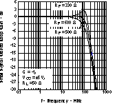
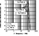
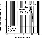
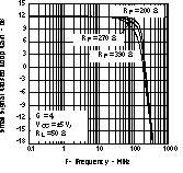
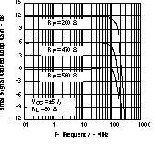
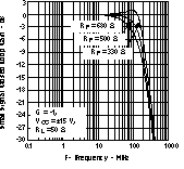
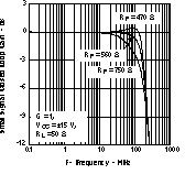
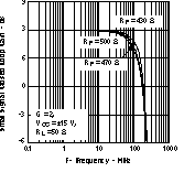
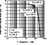
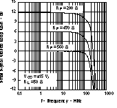
| Small-signal closed-loop gain | vs Frequency | Figure 1 to Figure 10 | |
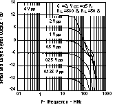
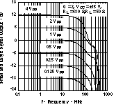
| Small- and large-signal output | vs Frequency | Figure 11, Figure 12 | |
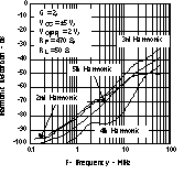
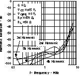
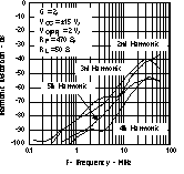
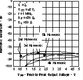
| Harmonic distortion | vs Frequency | Figure 13 to Figure 15 | |
| vs Peak-to-peak output voltage | Figure 16, Figure 17 | ||
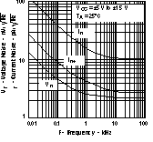
| Vn, In | Voltage noise and current noise | vs Frequency | Figure 18 |
| CMRR | Common-mode rejection ratio | vs Frequency | Figure 19 |
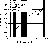
| Crosstalk | vs Frequency | Figure 20 | |
| Zo | Output impedance | vs Frequency | Figure 21 |
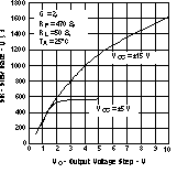
| SR | Slew rate | vs Output voltage step | Figure 22 |
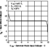
| VIO | Input offset voltage | vs Free-air temperature | Figure 24 |
| vs Common-mode input voltage | Figure 24 | ||
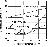
| IB | Input bias current | vs Free-air temperature | Figure 25 |
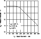
| VO | Output voltage | vs Load current | Figure 26 |
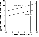
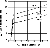
| Quiescent current | vs Free-air temperature | Figure 27 | |
| vs Supply voltage | Figure 28 | ||
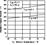
| ICC | Shutdown supply current | vs Free-air temperature | Figure 29 |
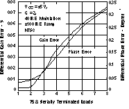
| Differential gain and phase error | vs 75-Ω serially terminated loads | Figure 30, Figure 31 | |
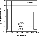
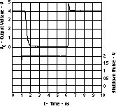
| Shutdown response | Figure 32 | ||
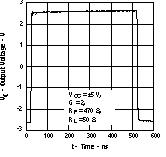
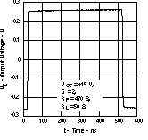
| Small-signal pulse response | Figure 33, Figure 34 | ||
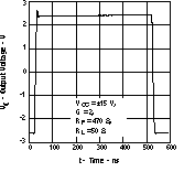
| Large-signal pulse response | Figure 35, Figure 36 | ||
7.12 Typical Characteristics
