SLOS382E September 2001 – May 2015 THS3122 , THS3125
PRODUCTION DATA.
- 1 Features
- 2 Applications
- 3 Description
- 4 Revision History
- 5 Device Options
- 6 Pin Configuration and Functions
-
7 Specifications
- 7.1 Absolute Maximum Ratings
- 7.2 Dissipation Ratings Table
- 7.3 Recommended Operating Conditions
- 7.4 Electrical Characteristics: Dynamic Performance
- 7.5 Electrical Characteristics: Noise and Distortion Performance
- 7.6 Electrical Characteristics: DC Performance
- 7.7 Electrical Characteristics: Input Characteristics
- 7.8 Electrical Characteristics: Output Characteristics
- 7.9 Electrical Characteristics: Power Supply
- 7.10 Electrical Characteristics: Shutdown Characteristics (THS3125 Only)
- 7.11 Typical Characteristics: Table Of Graphs
- 7.12 Typical Characteristics
- 8 Detailed Description
- 9 Application and Implementation
- 10Layout
- 11Device and Documentation Support
- 12Mechanical, Packaging, and Orderable Information
封装选项
机械数据 (封装 | 引脚)
散热焊盘机械数据 (封装 | 引脚)
- PWP|14
订购信息
8 Detailed Description
8.1 Overview
The THS3122 and THS3125 family of dual-channels, bipolar-input, high-speed current feedback amplifiers offers a low-noise of 2.2 nV/√Hz with a high output current drive of 450 mA. This performance is ideal for any application that requires low distortion over a wide range of frequencies with heavy loads.
8.2 Feature Description
8.2.1 Maximum Slew Rate For Repetitive Signals
The THS3125 and THS3122 are recommended for high slew rate pulsed applications where the internal nodes of the amplifier have time to stabilize between pulses. It is recommended to have at least 20-ns delay between pulses.
The THS3125 and THS3122 are not recommended for applications with repetitive signals (sine, square, sawtooth, or other) that exceed 900 V/µs. Using the part in these applications results in excessive current draw from the power supply and possible device damage.
For applications with high slew rate, repetitive signals, the THS3091 and THS3095 (single versions), or THS3092 and THS3096 (dual versions) are recommended.
8.2.2 Saving Power with Shutdown Functionality and Setting Threshold Levels with the Reference Pin
The THS3125 features a shutdown pin (SHUTDOWN) that lowers the quiescent current from 8.4 mA/amp down to 370 µA/amp, ideal for reducing system power.
The shutdown pin of the amplifier defaults to the REF pin voltage in the absence of an applied voltage, putting the amplifier in the normal on mode of operation. To turn off the amplifier in an effort to conserve power, the shutdown pin can be driven towards the positive rail. The threshold voltages for power-on and power-down (or shutdown) are relative to the supply rails and are given in the Electrical Characteristics: Shutdown Characteristics (THS3125 Only) table. Below the Enable threshold voltage, the device is on. Above the Disable threshold voltage, the device is off. Behavior between these threshold voltages is not specified.
Note that this shutdown functionality is self-defining: the amplifier consumes less power in shutdown mode. The shutdown mode is not intended to provide a high-impedance output. In other words, the shutdown functionality is not intended to allow use as a 3-state bus driver. When in shutdown mode, the impedance looking back into the output of the amplifier is dominated by the feedback and gain setting resistors, but the output impedance of the device itself varies depending on the voltage applied to the outputs.
As with most current feedback amplifiers, the internal architecture places some limitations on the system when in shutdown mode. Most notably is the fact that the amplifier actually turns on if there is a ±0.7 V or greater difference between the two input nodes (IN+ and IN–) of the amplifier. If this difference exceeds ±0.7 V, the output of the amplifier creates an output voltage equal to approximately [(IN+ – IN–) – 0.7V] × Gain. Also, if a voltage is applied to the output while in shutdown mode, the IN– node voltage is equal to VO(applied) × RG/(RF + RG) . For low gain configurations and a large applied voltage at the output, the amplifier may actually turn on because of the behavior described here.
The time delays associated with turning the device on and off are specified as the time it takes for the amplifier to reach either 10% or 90% of the final output voltage. The time delays are in the order of microseconds because the amplifier moves in and out of the linear mode of operation in these transitions.
8.2.3 Power-Down Reference Pin Operation
In addition to the shutdown pin, the THS3125 features a reference pin (REF) which allows the user to control the enable or disable power-down voltage levels applied to the SHUTDOWN pin. In most split-supply applications, the reference pin is connected to ground. In either case, the user must be aware of voltage-level thresholds that apply to the shutdown pin. Table 1 shows examples and illustrate the relationship between the reference voltage and the power-down thresholds. In the table, the threshold levels are derived by the following equations:
SHUTDOWN ≤ REF + 0.8 V for enable
SHUTDOWN ≥ REF + 2V for disable
Where the usable range at the REF pin is:
VCC– ≤ VREF ≤ (VCC+ – 4V)
The recommended mode of operation is to tie the REF pin to midrail, therefore setting the enable/disable thresholds to V(midrail) + 0.8 V and V(midrail) = 2 V, respectively.
Table 1. Shutdown Threshold Voltage Levels
| SUPPLY VOLTAGE (V) | REFERENCE PIN VOLTAGE (V) | ENABLE LEVEL (V) | DISABLE LEVEL (V) |
|---|---|---|---|
| ±15, ±5 | 0 | 0.8 | 2.0 |
| ±15 | 2.0 | 2.8 | 4.0 |
| ±15 | –2.0 | –1.2 | 0 |
| ±5 | 1.0 | 1.8 | 3.0 |
| ±5 | –1.0 | –0.2 | 1.0 |
| +30 | 15.0 | 15.8 | 17 |
| +10 | 5.0 | 5.8 | 7.0 |
Note that if the REF pin is left unterminated, it floats to the positive rail and falls outside of the recommended operating range given above VCC– ≤ VREF ≤ (VCC+ – 4V). As a result, it no longer serves as a reliable reference for the SHUTDOWN pin, and the enable/disable thresholds given above no longer apply. If the SHUTDOWN pin is also left unterminated, it floats to the positive rail and the device is disabled. If balanced, split supplies are used (±VS) and the REF and SHUTDOWN pins are grounded, the device is enabled.
8.3 Device Functional Modes
8.3.1 Wideband, Noninverting Operation
The THS3125 and THS3122 are unity gain stable 130-MHz current-feedback operational amplifiers, designed to operate from a ±5-V to ±15-V power supply.
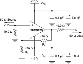
Figure 37 shows the THS3125 in a noninverting gain of 2-V/V configuration used to generate the typical characteristic curves. Most of the curves were characterized using signal sources with 50-Ω source impedance and with measurement equipment that presents a 50-Ω load impedance.
 Figure 37. Wideband, Noninverting Gain Configuration
Current-feedback amplifiers are highly dependent on the feedback resistor RF for maximum performance and stability. Table 2 shows the optimal gain setting resistors RF and RG at different gains to give maximum bandwidth with minimal peaking in the frequency response. Higher bandwidths can be achieved, at the expense of added peaking in the frequency response, by using even lower values for RF. Conversely, increasing RF decreases the bandwidth, but stability is improved.
Table 2. Recommended Resistor Values For Optimum Frequency Response
| THS3125 and THS3122 RF and RG VALUES FOR MINIMAL PEAKING WITH RL = 50 Ω, ±5-V to ±15-V POWER SUPPLY | ||
|---|---|---|
| GAIN (V/V) | RG (Ω) | RF (Ω) |
| 1 | — | 560 |
| 2 | 470 | 470 |
| 4 | 66.5 | 200 |
8.3.2 Wideband, Inverting Operation
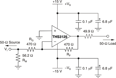
Figure 38 shows the THS3125 in a typical inverting gain configuration where the input and output impedances from Figure 37 are retained in an inverting circuit configuration.
 Figure 38. Wideband, Inverting Gain Configuration
8.3.3 Single-Supply Operation
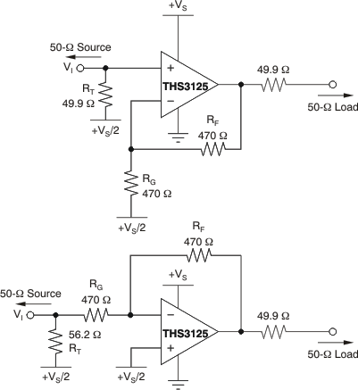
The THS3125 and THS3122 have the capability to operate from a single supply voltage ranging from 10 V to 30 V. When operating from a single power supply, biasing the input and output at mid-supply allows for the maximum output voltage swing. The circuits in Figure 39 show inverting and noninverting amplifiers configured for single-supply operation.
 Figure 39. DC-Coupled, Single-Supply Operation