ZHCSEP3B February 2016 – February 2016 THS3217
PRODUCTION DATA.
- 1 特性
- 2 应用
- 3 说明
- 4 修订历史记录
- 5 Device Comparison Table
- 6 Pin Configuration and Functions
-
7 Specifications
- 7.1 Absolute Maximum Ratings
- 7.2 ESD Ratings
- 7.3 Recommended Operating Conditions
- 7.4 Thermal Information
- 7.5 Electrical Characteristics: D2S
- 7.6 Electrical Characteristics: OPS
- 7.7 Electrical Characteristics: D2S + OPS
- 7.8 Electrical Characteristics: Midscale (DC) Reference Buffer
- 7.9 Typical Characteristics: D2S + OPS
- 7.10 Typical Characteristics: D2S Only
- 7.11 Typical Characteristics: OPS only
- 7.12 Typical Characteristics: Midscale (DC) Reference Buffer
- 7.13 Typical Characteristics: Switching Performance
- 7.14 Typical Characteristics: Miscellaneous Performance
- 8 Parameter Measurement Information
-
9 Detailed Description
- 9.1 Overview
- 9.2 Functional Block Diagram
- 9.3 Feature Description
- 9.4 Device Functional Modes
-
10Application and Implementation
- 10.1
Application Information
- 10.1.1
Typical Applications
- 10.1.1.1 High-Frequency, High-Voltage, Dual-Output Line Driver for AWGs
- 10.1.1.2 High-Voltage Pulse-Generator
- 10.1.1.3 Single-Supply, AC-Coupled, Piezo Element Driver
- 10.1.1.4 Output Common-Mode Control Using the Midscale Buffer as a Level Shifter
- 10.1.1.5 Differential I/O Driver With independent Common-Mode Control
- 10.1.1
Typical Applications
- 10.1
Application Information
- 11Power Supply Recommendations
- 12Layout
- 13器件和文档支持
- 14机械、封装和可订购信息
11 Power Supply Recommendations
The THS3217 typically operates on balanced, split supplies. The specifications and characterization plots use ±6 V in most cases. The full operating range for the THS3217 spans ±4 V to ±7.9 V. The input and output stages have separate supply pins that are isolated internally.
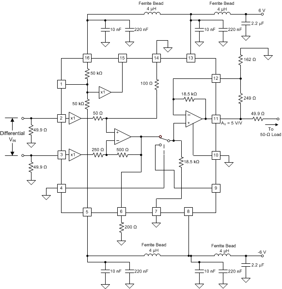
The recommended external supply configuration brings ±VCC into the output stage first, then back to the input stage connections through a π-filter comprised of ferrite beads and added decoupling capacitors at +VCC2 (pin 16) and –VCC2 (pin 5). Figure 106 shows an example decoupling configuration.
 Figure 106. Recommended Power-Supply Configuration
The ferrite bead acts to break the feedback loop from the output stage load currents back into the D2S and midscale buffer stages. Operate the two positive supply pins and the two negative supply pins at the same voltage. Using separate sources on the two pins risks forward-biasing the on-chip parallel diodes connecting the two supply inputs together. +VCC1 (pin 13) and +VCC2 (pin 16) have two parallel diodes that are normally off if the voltage at the two pins are equal. The same is true for –VCC1 (pin 8) and –VCC2 (pin 5).
The THS3217 provides considerable flexibility in the supply voltage settings. The overriding consideration is always satisfying the required headroom to the supplies on all the I/O paths. The logic controls on PATHSEL (pin 4) and DISABLE (pin 10) are intended to operate ground referenced regardless of supplies used. The ground connection on pin 7 is used to set the reference.
Power savings are certainly possible by operating with only the minimum required supplies for the intended swings at each of the pins. For instance, consider an example design operating with a current-sinking DAC with the input common-mode voltage at 3 V, with an output swing at the D2S output of ±1 V. Looking at just the D2S stage under these conditions, the minimum positive supply is 3 VCM + the maximum input headroom of 1.5 V to the positive supply, resulting in a minimum 4.5-V supply for this operation. The ±1-V output at VO1 (pin 6) along with the D2S output headroom sets the minimum negative supply voltage. The maximum 1.65-V headroom gives a possible minimum negative supply of –2.65 V. However, the minimum operating total of 8 V increases the negative supply to –3.5 V.
If the ±1-V swing is then amplified by the OPS, the output swing and headroom requirements set the minimum operating supply. For instance, if the OPS is operating at a gain of 2.5 V/V, the ±2.5-V output requires a maximum headroom of 1.4 V to either supply. Achieving a 1.4-V headroom requires a minimum balanced supply of ±3.9 V. However, the input stage overrides the positive side because the required minimum is 4.5 V, while the negative increases to –3.9 V. This example of absolute minimum supplies saves power. Using a typical 56-mA quiescent current for all stages, going to the minimum 8.4 V total across the device, uses 470 mW of quiescent power versus the 672 mW if a simple ±6-V supply is applied. However, ac performance degrades with the lower headroom. For more power-sensitive applications, consider adjusting the supplies to the minimum required on each side.
11.1 Thermal Considerations
The internal power for the THS3217 is a combination of its quiescent power and load power. The quiescent power is simply the total supply voltage times the supply current. This current is trimmed to reduce power dissipation variation and minimize variations in the ac performance. At a ±7.5-V supply, the maximum supply current of 57 mA dissipates 855 mW of quiescent power. The worst-case load power occurs if the output is at ½ the single-sided supply voltage driving a dc load. Placing a ±3.75-V dc output into 100 Ω adds another 37.5 mA × 3.75 V = 140 mW of internal power. This total of approximately 1 W of internal dissipation requires the thermal pad be connected to a good heat-spreading ground plane to hold the internal junction temperatures below the rated maximum of 150°C.
The thermal impedance is approximately 45 °C/W with the thermal pad connected. For 1 W of internal power dissipation there is a 45°C (approximate) rise in the junction temperature from ambient. Designing for the intended 85°C maximum ambient temperature results in a maximum junction temperature of 130°C.