ZHCSHX6C August   2017  – February 2023 THS3491

PRODUCTION DATA  

  1. 特性
  2. 应用
  3. 说明
  4. Revision History
  5. Device Comparison Table
  6. Pin Configuration and Functions
  7. Bare Die Information
  8. Specifications
    1. 8.1 Absolute Maximum Ratings
    2. 8.2 ESD Ratings
    3. 8.3 Recommended Operating Conditions
    4. 8.4 Thermal Information
    5. 8.5 Electrical Characteristics: VS = ±15 V
    6. 8.6 Electrical Characteristics: VS = ±7.5 V
    7. 8.7 Typical Characteristics: ±15 V
    8. 8.8 Typical Characteristics: ±7.5 V
  9. Detailed Description
    1. 9.1 Overview
    2. 9.2 Functional Block Diagram
    3. 9.3 Feature Description
      1. 9.3.1 Power-Down (PD) Pin
      2. 9.3.2 Power-Down Reference (REF) Pin
      3. 9.3.3 Internal Junction Temperature Sense (TJ_SENSE) Pin
    4. 9.4 Device Functional Modes
      1. 9.4.1 Wideband Noninverting Operation
      2. 9.4.2 Wideband, Inverting Operation
      3. 9.4.3 Single-Supply Operation
      4. 9.4.4 Maximum Recommended Output Voltage
  10. 10Application and Implementation
    1. 10.1 Application Information
      1. 10.1.1 Driving Capacitive Loads
      2. 10.1.2 Video Distribution
    2. 10.2 Typical Application
      1. 10.2.1 Design Requirements
      2. 10.2.2 Detailed Design Procedure
      3. 10.2.3 Application Curves
    3. 10.3 Power Supply Recommendations
    4. 10.4 Layout
      1. 10.4.1 Layout Guidelines
        1. 10.4.1.1 PowerPAD™ Integrated Circuit Package Design Considerations (DDA Package Only)
          1. 10.4.1.1.1 PowerPAD™ Integrated Circuit Package Layout Considerations
          2. 10.4.1.1.2 Power Dissipation and Thermal Considerations
      2. 10.4.2 Layout Example
  11. 11Device and Documentation Support
    1. 11.1 Documentation Support
      1. 11.1.1 Related Documentation
    2. 11.2 接收文档更新通知
    3. 11.3 支持资源
    4. 11.4 Trademarks
    5. 11.5 静电放电警告
    6. 11.6 术语表
  12. 12Mechanical, Packaging, and Orderable Information

封装选项

机械数据 (封装 | 引脚)
散热焊盘机械数据 (封装 | 引脚)
订购信息

Typical Application

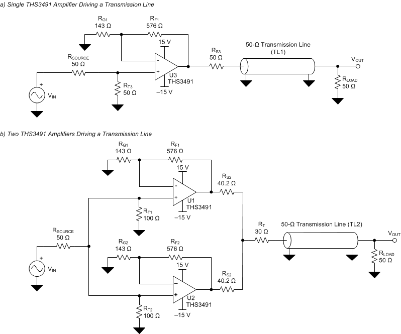
The fundamental concept of load sharing is to drive a load using two or more of the same operational amplifier. Each amplifier is driven by the same source. Figure 10-5 shows two THS3491 amplifiers sharing the same load. This concept effectively reduces the current load of each amplifier by 1/N, where N is the number of amplifiers.
GUID-AE4C00E9-1E73-43B1-8119-34FA537742EE-low.gif Figure 10-5 Load-Sharing Driver Application