ZHCSPA5F August 1999 – July 2024 THS4021 , THS4022
PRODUCTION DATA
- 1
- 1 特性
- 2 应用
- 3 说明
- 4 Pin Configuration and Functions
-
5 Specifications
- 5.1 Absolute Maximum Ratings
- 5.2 ESD Ratings
- 5.3 Recommended Operating Conditions
- 5.4 Thermal Information - THS4021
- 5.5 Thermal Information - THS4022
- 5.6 Electrical Characteristics - THS4021D and THS4022DGN
- 5.7 Electrical Characteristics - THS4021DGN
- 5.8 Typical Characteristics: THS4021D and THS4022DGN
- 5.9 Typical Characteristics: THS4021DGN
- 6 Detailed Description
- 7 Application and Implementation
- 8 Device and Documentation Support
- 9 Revision History
- 10Mechanical, Packaging, and Orderable Information
封装选项
请参考 PDF 数据表获取器件具体的封装图。
机械数据 (封装 | 引脚)
- D|8
- DGN|8
散热焊盘机械数据 (封装 | 引脚)
- DGN|8
订购信息
7.3.1.1 General PowerPAD™ Integrated Circuit Package Design Considerations
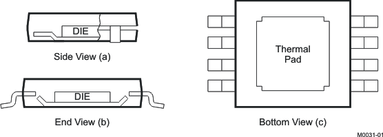
The THS402x is available in a thermally-enhanced DGN package, which is a member of the PowerPAD™ integrated circuit package family. Figure 7-3a and Figure 7-3b show that this package is constructed using a downset leadframe upon which the die is mounted. Figure 7-3c that this arrangement results in the leadframe being exposed as a thermal pad on the underside of the package. Because this thermal pad has direct thermal contact with the die, excellent thermal performance can be achieved by providing a good thermal path away from the thermal pad.
The PowerPAD integrated circuit package allows for both assembly and thermal management in one manufacturing operation. During the surface-mount solder operation (when the leads are being soldered), the thermal pad can also be soldered to a copper area underneath the package. Through the use of thermal paths within this copper area, heat can be conducted away from the package into either a ground plane or other heat dissipating device.
The PowerPAD integrated circuit package represents a breakthrough in combining the small area and ease of assembly of the surface mount with the previously awkward mechanical methods of heat sinking.
More complete details of the PowerPAD installation process and thermal management techniques are found in PowerPAD Thermally-Enhanced Package. This document is found on the TI website (www.ti.com) by searching on the keyword PowerPAD. The document can also be ordered through your local TI sales office; refer to SLMA002 when ordering.
