ZHCSPA5F August 1999 – July 2024 THS4021 , THS4022
PRODUCTION DATA
- 1
- 1 特性
- 2 应用
- 3 说明
- 4 Pin Configuration and Functions
-
5 Specifications
- 5.1 Absolute Maximum Ratings
- 5.2 ESD Ratings
- 5.3 Recommended Operating Conditions
- 5.4 Thermal Information - THS4021
- 5.5 Thermal Information - THS4022
- 5.6 Electrical Characteristics - THS4021D and THS4022DGN
- 5.7 Electrical Characteristics - THS4021DGN
- 5.8 Typical Characteristics: THS4021D and THS4022DGN
- 5.9 Typical Characteristics: THS4021DGN
- 6 Detailed Description
- 7 Application and Implementation
- 8 Device and Documentation Support
- 9 Revision History
- 10Mechanical, Packaging, and Orderable Information
封装选项
请参考 PDF 数据表获取器件具体的封装图。
机械数据 (封装 | 引脚)
- D|8
- DGN|8
散热焊盘机械数据 (封装 | 引脚)
- DGN|8
订购信息
7.1.1 Driving a Capacitive Load
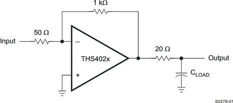
The THS402x are internally compensated to maximize bandwidth and slew-rate performance. To maintain stability, take additional precautions when driving capacitive loads with a high-performance amplifier. As a result of the internal compensation, significant capacitive loading directly on the output node decreases the device phase margin, and potentially lead to high-frequency ringing or oscillations. Therefore, for capacitive loads greater than 10 pF, place an isolation resistor in series with the output of the amplifier. Figure 7-1 shows this configuration. For most applications, a minimum resistance of 20 Ω is recommended. In 75‑Ω transmission systems, setting the series resistor value to 75 Ω is a beneficial choice because this value isolates any capacitance loading and provides source impedance matching.
 Figure 7-1 Driving a
Capacitive Load