SLOS432B April 2004 – October 2015 THS4281
PRODUCTION DATA.
- 1 Features
- 2 Applications
- 3 Description
- 4 Revision History
- 5 Pin Configuration and Functions
-
6 Specifications
- 6.1 Absolute Maximum Ratings
- 6.2 ESD Ratings
- 6.3 Recommended Operating Conditions
- 6.4 Thermal Information
- 6.5 Electrical Characteristics, VS = 3 V (VS+ = 3 V, VS- = GND)
- 6.6 Electrical Characteristics, VS = 5 V (VS+ = 5 V, VS- = GND)
- 6.7 Electrical Characteristics, VS = ±5 V
- 6.8 Dissipation Ratings
- 6.9 Typical Characteristics
- 7 Detailed Description
- 8 Application and Implementation
- 9 Power Supply Recommendations
- 10Layout
- 11Device and Documentation Support
- 12Mechanical, Packaging, and Orderable Information
封装选项
请参考 PDF 数据表获取器件具体的封装图。
机械数据 (封装 | 引脚)
- D|8
- DBV|5
- DGK|8
散热焊盘机械数据 (封装 | 引脚)
订购信息
7 Detailed Description
7.1 Overview
7.2 Feature Description
7.2.1 Wideband, Noninverting Operation
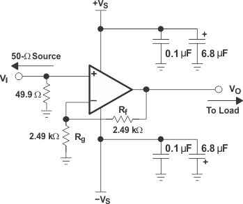
Figure 68 shows the noninverting gain configuration of 2 V/V used to demonstrate the typical performance curves.
Voltage feedback amplifiers can use a wide range of resistors values to set their gain with minimal impact on frequency response. Larger-valued resistors decrease loading of the feedback network on the output of the amplifier, but may cause peaking and instability. For a gain of +2, feedback resistor values between 1 kΩ and 4 kΩ are recommended for most applications. However, as the gain increases, the use of even higher feedback resistors can be used to conserve power. This is due to the inherent nature of amplifiers becoming more stable as the gain increases, at the expense of bandwidth. Figure 73 and Figure 74 show the THS4281 using feedback resistors of 10 kΩ and 100 kΩ. Be cautioned that using such high values with high-speed amplifiers is not typically recommended, but under certain conditions, such as high gain and good high-speed printed circuit board (PCB) layout practices, such resistances can be used.
 Figure 68. Wideband, Noninverting Gain Configuration
7.2.2 Wideband, Inverting Operation
Figure 69 shows a typical inverting configuration where the input and output impedances and noise gain from Figure 68 are retained with an inverting circuit gain of –1 V/V.
 Figure 69. Wideband, Inverting Gain Configuration
In the inverting configuration, some key design considerations must be noted. One is that the gain resistor (Rg) becomes part of the signal channel input impedance. If the input impedance matching is desired (which is beneficial whenever the signal is coupled through a cable, twisted pair, long PCB trace, or other transmission line conductors), Rg may be set equal to the required termination value and Rf adjusted to give the desired gain. However, care must be taken when dealing with low inverting gains, as the resulting feedback resistor value can present a significant load to the amplifier output. For example, an inverting gain of 2, setting Rg to 49.9 Ω for input matching, eliminates the need for RM but requires a 100-Ω feedback resistor. The 100-Ω feedback resistor, in parallel with the external load, causes excessive loading on the amplifier output. To eliminate this excessive loading, it is preferable to increase both Rg and Rf values, as shown in Figure 69, and then achieve the input matching impedance with a third resistor (RM) to ground. The total input impedance is the parallel combination of Rg and RM.
Another consideration in inverting amplifier design is setting the bias current cancellation resistor (RT) on the noninverting input. If the resistance is set equal to the total dc resistance presented to the device at the inverting terminal, the output dc error (due to the input bias currents) is reduced to the input offset current multiplied by RT. In Figure 69, the dc source impedance presented at the inverting terminal is 2.49 kΩ || (2.49 kΩ + 25.3 Ω) ≈ 1.24 kΩ. To reduce the additional high-frequency noise introduced by the resistor at the noninverting input, RT is bypassed with a 0.1-μF capacitor to ground (CT).
7.3 Device Functional Modes
This device has no specific function modes.