SLOS432B April 2004 – October 2015 THS4281
PRODUCTION DATA.
- 1 Features
- 2 Applications
- 3 Description
- 4 Revision History
- 5 Pin Configuration and Functions
-
6 Specifications
- 6.1 Absolute Maximum Ratings
- 6.2 ESD Ratings
- 6.3 Recommended Operating Conditions
- 6.4 Thermal Information
- 6.5 Electrical Characteristics, VS = 3 V (VS+ = 3 V, VS- = GND)
- 6.6 Electrical Characteristics, VS = 5 V (VS+ = 5 V, VS- = GND)
- 6.7 Electrical Characteristics, VS = ±5 V
- 6.8 Dissipation Ratings
- 6.9 Typical Characteristics
- 7 Detailed Description
- 8 Application and Implementation
- 9 Power Supply Recommendations
- 10Layout
- 11Device and Documentation Support
- 12Mechanical, Packaging, and Orderable Information
封装选项
请参考 PDF 数据表获取器件具体的封装图。
机械数据 (封装 | 引脚)
- D|8
- DBV|5
- DGK|8
散热焊盘机械数据 (封装 | 引脚)
订购信息
5 Pin Configuration and Functions
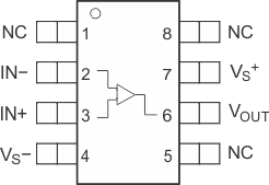
D and DGK Packages
8-Pin SOIC
Top View

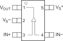
DBV Package
5-Pin SOT-23
Top View

NOTE:
NC Indicates there is no internal connection to these pinsPin Functions
| PIN | I/O | DESCRIPTION | ||
|---|---|---|---|---|
| NAME | SOIC, VSSOP | SOT-23 | ||
| NC | 1 | — | — | |
| IN- | 2 | 4 | I | Negative input voltage pin |
| IN+ | 3 | 3 | I | Positive input voltage pin |
| Vs- | 4 | 2 | I/O | Negative supply input voltage pin |
| NC | 5 | — | — | |
| Vout | 6 | 1 | O | Output voltage pin |
| Vs+ | 7 | 5 | I/O | Postive supply input voltage pin |
| NC | 8 | — | — | |