SLOS454I January 2005 – July 2016 THS4509
PRODUCTION DATA.
- 1 Features
- 2 Applications
- 3 Description
- 4 Revision History
- 5 Device Comparison Table
- 6 Pin Configuration and Functions
- 7 Specifications
- 8 Detailed Description
- 9 Application and Implementation
- 10Power Supply Recommendations
- 11Layout
- 12Device and Documentation Support
- 13Mechanical, Packaging, and Orderable Information
8 Detailed Description
8.1 Overview
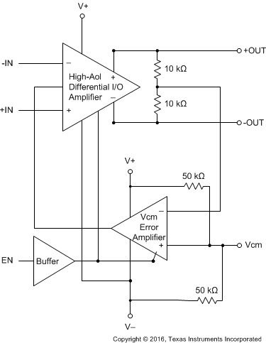
The THS4509 is a fully differential amplifier with integrated common-mode control designed to provide low distortion amplification to wide bandwidth differential signals. The common-mode feedback circuit sets the output common-mode voltage independent of the input common mode, as well as forcing the V+ and V − outputs to be equal in magnitude and opposite in phase, even when only one of the inputs is driven as in single to differential conversion.
8.2 Functional Block Diagram
8.3 Feature Description
8.3.1 Test Circuits
The THS4509 is tested with the following test circuits built on the evaluation module (EVM). For simplicity, power-supply decoupling is not shown—see Layout for recommendations. Depending on the test conditions, component values are changed per Table 3 and Table 4, or as otherwise noted. The signal generators used are AC-coupled, 50-Ω sources, and a 0.22-μF capacitor and 49.9-Ω resistor to ground are inserted across RIT on the alternate input to balance the circuit. A split power supply is used to ease the interface to common test equipment, but the amplifier can be operated single-supply as described in Typical Applications with no impact on performance.
Table 3. Gain Component Values
| GAIN | RF | RG | RIT |
|---|---|---|---|
| 6 dB | 348 Ω | 165 Ω | 61.9 Ω |
| 10 dB | 348 Ω | 100 Ω | 69.8 Ω |
| 14 dB | 348 Ω | 56.2 Ω | 88.7 Ω |
| 20 dB | 348 Ω | 16.5 Ω | 287 Ω |
Note the gain setting includes 50-Ω source impedance. Components are chosen to achieve gain and 50-Ω input termination.
Table 4. Load Component Values
| RL | RO | ROT | ATTEN. |
|---|---|---|---|
| 100 Ω | 25 Ω | Open | 6 dB |
| 200 Ω | 86.6 Ω | 69.8 Ω | 16.8 dB |
| 499 Ω | 237 Ω | 56.2 Ω | 25.5 dB |
| 1k Ω | 487 Ω | 52.3 Ω | 31.8 dB |
Note the total load includes 50-Ω termination by the test equipment. Components are chosen to achieve load and 50-Ω line termination through a 1:1 transformer.
Due to the voltage divider on the output formed by the load component values, the amplifier output is attenuated. The column Atten in Table 4 shows the attenuation expected from the resistor divider. When using a transformer at the output as shown in Figure 77, the signal sees slightly more loss, and these numbers are approximate.
8.3.1.1 Frequency Response
The circuit shown in Figure 76 is used to measure the frequency response of the circuit.
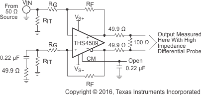 Figure 76. Frequency Response Test Circuit
A network analyzer is used as the signal source and as the measurement device. The output impedance of the network analyzer is 50 Ω. RIT and RG are chosen to impedance match to 50 Ω, and to maintain the proper gain. To balance the amplifier, a 0.22-μF capacitor and 49.9-Ω resistor to ground are inserted across RIT on the alternate input.
The output is probed using a high-impedance differential probe across the 100-Ω resistor. The gain is referred to the amplifier output by adding back the 6-dB loss due to the voltage divider on the output.
8.3.1.2 Distortion and 1-dB Compression
The circuit shown in Figure 77 is used to measure harmonic distortion, intermodulation distortion, and 1-db compression point of the amplifier.
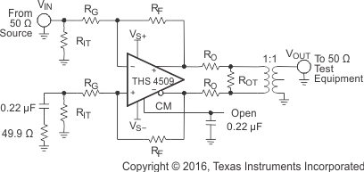 Figure 77. Distortion Test Circuit
A signal generator is used as the signal source and the output is measured with a spectrum analyzer. The output impedance of the signal generator is 50 Ω. RIT and RG are chosen to impedance-match to 50 Ω, and to maintain the proper gain. To balance the amplifier, a 0.22-μF capacitor and 49.9-Ω resistor to ground are inserted across RIT on the alternate input.
A low-pass filter is inserted in series with the input to reduce harmonics generated at the signal source. The level of the fundamental is measured, then a high-pass filter is inserted at the output to reduce the fundamental so that it does not generate distortion in the input of the spectrum analyzer.
The transformer used in the output to convert the signal from differential to single-ended is an ADT1-1WT. It limits the frequency response of the circuit so that measurements cannot be made below approximately 1 MHz.
The 1-dB compression point is measured with a spectrum analyzer with 50-Ω double termination or 100-Ω termination; see Table 4. The input power is increased until the output is 1 dB lower than expected. The number reported in the table data is the power delivered to the spectrum analyzer input. Add 3 dB to refer to the amplifier output.
8.3.1.3 S-Parameter, Slew Rate, Transient Response, Settling Time, Output Impedance, Overdrive, Output Voltage, Turnon, and Turnoff Time
The circuit shown in Figure 78 is used to measure s-parameters, slew rate, transient response, settling time, output impedance, overdrive recovery, output voltage swing, turnon, and turnoff times of the amplifier. For output impedance, the signal is injected at VOUT with VIN left open and the drop across the 49.9-Ω resistor is used to calculate the impedance seen looking into the amplifier output.
Because S21 is measured single-ended at the load with 50-Ω double termination, add 12 dB to refer to the amplifier output as a differential signal.
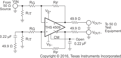 Figure 78. S-Parameter, SR, Transient Response, Settling Time, ZO, Overdrive Recovery, VOUT Swing, Turnon, and Turnoff Test Circuit
8.3.1.4 CM Input
The circuit shown in Figure 79 is used to measure the frequency response and input impedance of the CM input. Frequency response is measured single-ended at VOUT+ or VOUT– with the input injected at VIN, RCM = 0 Ω, and RCMT = 49.9 Ω. The input impedance is measured with RCM = 49.9 Ω with RCMT = open, and calculated by measuring the voltage drop across RCM to determine the input current.
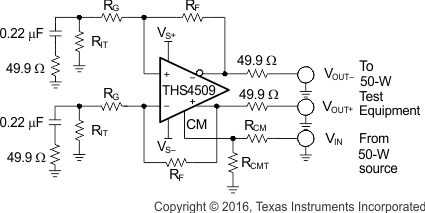 Figure 79. CM Input Test Circuit
8.3.1.5 CMRR and PSRR
The circuit shown in Figure 80 is used to measure the CMRR and PSRR of VS+ and VS–. The input is switched appropriately to match the test being performed.
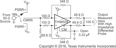 Figure 80. CMRR and PSRR Test Circuit
8.4 Device Functional Modes
The THS4509 has one main functional mode with two variants. The amplifier functions as either a differential to differential or a single-ended to differential amplifier. In either of these modes the amplifier output operating point (common-mode voltage) is set independently by the CM pin.
The THS4509 also features a power-down state for reduced power consumption when the amplifier is not required to be operational.