SBOS458H December 2008 – June 2015 THS4521 , THS4522 , THS4524
PRODUCTION DATA.
- 1 Features
- 2 Applications
- 3 Description
- 4 Revision History
- 5 Device Comparison Table
- 6 Pin Configuration and Functions
-
7 Specifications
- 7.1 Absolute Maximum Ratings
- 7.2 ESD Ratings
- 7.3 Recommended Operating Conditions
- 7.4 Thermal Information
- 7.5 Electrical Characteristics: VS+ - VS- = 3.3 V
- 7.6 Electrical Characteristics: VS+ - VS- = 5 V
- 7.7 Typical Characteristics
- 7.8 Typical Characteristics: VS+ - VS- = 3.3 V
- 7.9 Typical Characteristics: 5 V
-
8 Detailed Description
- 8.1 Overview
- 8.2 Functional Block Diagram
- 8.3
Feature Description
- 8.3.1 Frequency Response
- 8.3.2 Distortion
- 8.3.3 Slew Rate, Transient Response, Settling Time, Output Impedance, Overdrive, Output Voltage, and Turn-On/Turn-Off Time
- 8.3.4 Common-Mode and Power-Supply Rejection
- 8.3.5 VOCM Input
- 8.3.6 Typical Performance Variation With Supply VoltageTypical Performance Variation with Supply Voltage section
- 8.3.7 title of Single-Supply Operation sectionSingle-Supply Operation
- 8.3.8 Low-Power Applications and the Effects of Resistor Values on Bandwidth
- 8.3.9 Frequency Response Variation due to Package Options
- 8.3.10 Driving Capacitive Loads
- 8.3.11 Audio Performance
- 8.3.12 Audio On/Off Pop Performance
- 8.4
Device Functional Modes
- 8.4.1
Operation from Single-Ended Sources to Differential Outputs
- 8.4.1.1 AC-Coupled Signal Path Considerations for Single-Ended Input to Differential Output Conversion
- 8.4.1.2 DC-Coupled Input Signal Path Considerations for Single-Ended to Differential Conversion
- 8.4.1.3 Resistor Design Equations for the Single-Ended to Differential Configuration of the FDA
- 8.4.1.4 Input Impedance for the Single-Ended to Differential FDA Configuration
- 8.4.2 Differential-Input to Differential-Output Operation
- 8.4.1
Operation from Single-Ended Sources to Differential Outputs
- 8.5 Programming
-
9 Application and Implementation
- 9.1 Application Information
- 9.2 Typical Applications
- 10Power Supply Recommendations
- 11Layout
- 12Device and Documentation Support
- 13Mechanical, Packaging, and Orderable Information
11 Layout
11.1 Layout Guidelines
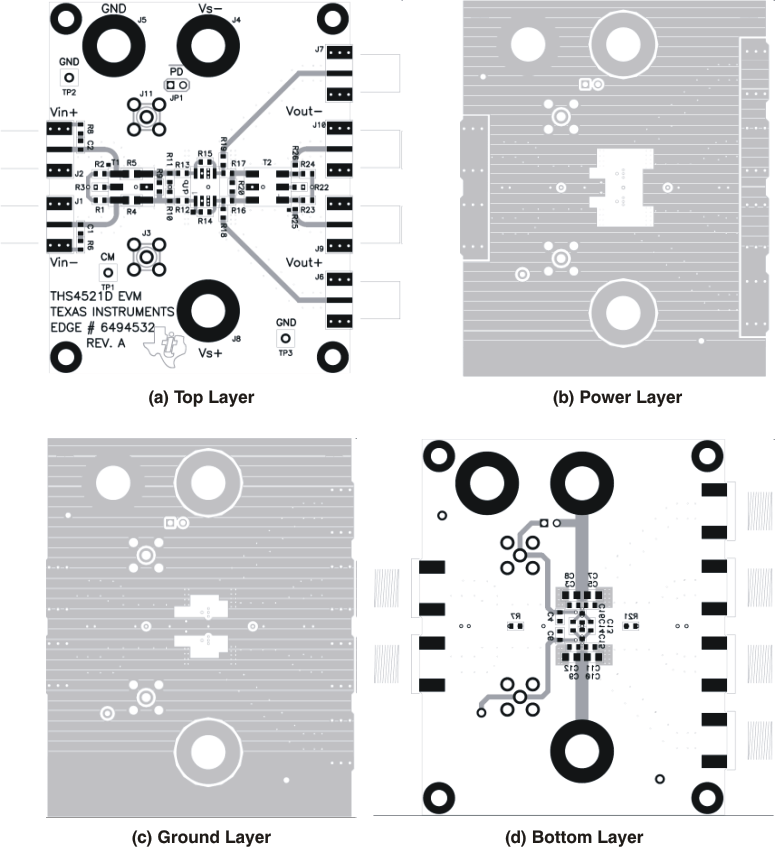
Figure 80 shows the THS4521EVM schematic. PCB layers 1 through 4 are shown in Figure 93; Table 9 lists the bill of materials for the THS4521EVM as supplied from TI. It is recommended to follow the layout of the external components near to the amplifier, ground plane construction, and power routing as closely as possible. Follow these general guidelines:
- Signal routing should be direct and as short as possible into and out of the amplifier circuit.
- The feedback path should be short and direct.
- Ground or power planes should be removed from directly under the amplifier input and output pins.
- An output resistor is recommended in each output lead, placed as near to the output pins as possible.
- Two 0.1-μF power-supply decoupling capacitors should be placed as near to the power-supply pins as possible.
- Two 10-μF power-supply decoupling capacitors should be placed within 1 inch of the device and can be shared among multiple analog devices.
- A 0.22-μF capacitor should be placed between the VOCM input pin and ground near to the pin. This capacitor limits noise coupled into the pin.
- The PD pin uses TTL logic levels; a bypass capacitor is not necessary if actively driven, but can be used for robustness in noisy environments whether driven or not.
- If input termination resistors R10 and R11 are used, a single point connection to ground on L2 is recommended.
11.2 Layout Example
 Figure 93. THS4521EVM: Layer 1 to Layer 4 Images