SBOS458H December 2008 – June 2015 THS4521 , THS4522 , THS4524
PRODUCTION DATA.
- 1 Features
- 2 Applications
- 3 Description
- 4 Revision History
- 5 Device Comparison Table
- 6 Pin Configuration and Functions
-
7 Specifications
- 7.1 Absolute Maximum Ratings
- 7.2 ESD Ratings
- 7.3 Recommended Operating Conditions
- 7.4 Thermal Information
- 7.5 Electrical Characteristics: VS+ - VS- = 3.3 V
- 7.6 Electrical Characteristics: VS+ - VS- = 5 V
- 7.7 Typical Characteristics
- 7.8 Typical Characteristics: VS+ - VS- = 3.3 V
- 7.9 Typical Characteristics: 5 V
-
8 Detailed Description
- 8.1 Overview
- 8.2 Functional Block Diagram
- 8.3
Feature Description
- 8.3.1 Frequency Response
- 8.3.2 Distortion
- 8.3.3 Slew Rate, Transient Response, Settling Time, Output Impedance, Overdrive, Output Voltage, and Turn-On/Turn-Off Time
- 8.3.4 Common-Mode and Power-Supply Rejection
- 8.3.5 VOCM Input
- 8.3.6 Typical Performance Variation With Supply VoltageTypical Performance Variation with Supply Voltage section
- 8.3.7 title of Single-Supply Operation sectionSingle-Supply Operation
- 8.3.8 Low-Power Applications and the Effects of Resistor Values on Bandwidth
- 8.3.9 Frequency Response Variation due to Package Options
- 8.3.10 Driving Capacitive Loads
- 8.3.11 Audio Performance
- 8.3.12 Audio On/Off Pop Performance
- 8.4
Device Functional Modes
- 8.4.1
Operation from Single-Ended Sources to Differential Outputs
- 8.4.1.1 AC-Coupled Signal Path Considerations for Single-Ended Input to Differential Output Conversion
- 8.4.1.2 DC-Coupled Input Signal Path Considerations for Single-Ended to Differential Conversion
- 8.4.1.3 Resistor Design Equations for the Single-Ended to Differential Configuration of the FDA
- 8.4.1.4 Input Impedance for the Single-Ended to Differential FDA Configuration
- 8.4.2 Differential-Input to Differential-Output Operation
- 8.4.1
Operation from Single-Ended Sources to Differential Outputs
- 8.5 Programming
-
9 Application and Implementation
- 9.1 Application Information
- 9.2 Typical Applications
- 10Power Supply Recommendations
- 11Layout
- 12Device and Documentation Support
- 13Mechanical, Packaging, and Orderable Information
9 Application and Implementation
NOTE
Information in the following applications sections is not part of the TI component specification, and TI does not warrant its accuracy or completeness. TI’s customers are responsible for determining suitability of components for their purposes. Customers should validate and test their design implementation to confirm system functionality.
9.1 Application Information
The following circuits show application information for the THS4521, THS4522, and THS4524 family. For simplicity, power-supply decoupling capacitors are not shown in these diagrams; see Layout Guidelines for suggested guidelines. For more details on the use and operation of fully differential amplifiers, refer to the Application Report Fully-Differential Amplifiers(SLOA054), available for download from the TI web site at www.ti.com.
9.2 Typical Applications
9.2.1 Audio ADC Driver Performance: THS4521 and PCM4204 Combined Performance
To show achievable performance with a high-performance audio ADC, the THS4521 is tested as the drive amplifier for the PCM4204. The PCM4204 is a high-performance, four-channel ADC designed for professional and broadcast audio applications. The PCM4204 architecture uses a 1-bit delta-sigma (ΔΣ) modulator per channel that incorporates an advanced dither scheme for improved dynamic performance, and supports PCM output data. The PCM4204 provides a flexible serial port interface and many other advanced features. Refer to the PCM4204 product data sheet for more information.
The PCM4204EVM can test the audio performance of the THS4521 as a drive amplifier. The standard PCM4204EVM is provided with four OPA1632 fully-differential amplifiers, which use the same device pinout as the THS4521. For testing, one of these amplifiers is replaced with a THS4521 device in same package (MSOP), and the power supply changes to a single-supply +5V. Figure 79 shows the modifications made to the circuit. Note the resistor connecting the VOCM input of the THS4521 to the input common-mode drive from the PCM4204 is shown removed and is optional; no performance change was noted with it connected or removed. The THS4521 is operated with a +5-V single-supply so the output common-mode defaults to +2.5 V as required at the input of the PCM4204. The EVM power connections were modified by connecting positive supply inputs, +15 V, +5 VA and +5 VD, to a +5-V external power supply (EXT +3.3 was not used) and connecting –15 V and all ground inputs to ground on the external power supply. Note only one external +5-V supply was needed to power all devices on the EVM.
A SYS-2722 Audio Analyzer from Audio Precision (AP) provides an analog audio input to the EVM; the PCM-formatted digital output is read by the digital input on the AP.
Data were taken using a 256-fS system clock to achieve fS = 48-kHz measurements, and audio output uses PCM format. Other data rates and formats are expected to show similar performance in line with that shown in the product data sheet.
Figure 82 shows the THD+N vs Frequency response with no weighting; Figure 83 shows an FFT of the output with 1-kHz input tone. Input signals to the PCM4204 for these tests is 0.5 dBFS. Dynamic range is also tested at –60 dBFS, fIN = 1 kHz, and A-weighted. Table 8 summarizes testing results using the THS4521 together with the PCM4204 versus typical data sheet performance measurements, and show that it make an excellent drive amplifier for this ADC.
The test circuit shown in Figure 79 has a gain = 0.27 and attenuates the input signal. For applications that require higher gain, the circuit was modified to gains of G = 1, G = 2, and G = 5 by replacing the feedback resistors (R33 and R34) and re-tested to show performance.
Figure 84 shows the THS4521 and PCM4204 THD+N versus frequency with no weighting at higher gains.
9.2.1.1 Design Requirements
Table 8. 1-kHz AC Analysis: Test Circuit Versus PCM4204 Data Sheet Typical Specifications
(FS = 48 kSPS)
| Configuration | Tone | THD+N | Dynamic Range |
|---|---|---|---|
| THS4521 and PCM4204 | 1 kHz | –106 dBc | 117 dB |
| PCM4204 Data sheet (typ) | 1 kHz | –105 dBc | 118 dB |
9.2.1.2 Detailed Design Procedure
Table 9. THS4521EVM Parts List
| ITEM | DESCRIPTION | SMD SIZE | REFERENCE DESIGNATOR |
QTY | MANUFACTURER PART NUMBER |
|---|---|---|---|---|---|
| 1 | Capacitor, 10.0 μF, ceramic, X5R, 6.3 V | 0805 | C7, C8, C9, C10 | 4 | (AVX) 08056D106KAT2A |
| 2 | Capacitor, 0.1 μF, ceramic, X7R, 16 V | 0603 | C3, C5, C11, C12 | 4 | (AVX) 0603YC104KAT2A |
| 3 | Capacitor, 0.22 μF, ceramic, X7R, 10 V | 0603 | C1, C4, C6 | 3 | (AVX) 0603ZC224KAT2A |
| 4 | Open | 0603 | C2, C13, C14, C15, C16 | 5 | |
| 5 | Open | 0603 | R1, R2, R3, R7, R8, R9, R18, R19, R21, R22, R23, R26 | 12 | |
| 6 | Resistor, 0 Ω | 0603 | R24, R25 | 2 | (ROHM) MCR03EZPJ000 |
| 7 | Resistor, 49.9 Ω, 1/10W, 1% | 0603 | R6 | 1 | (ROHM) MCR03EZPFX49R9 |
| 8 | Resistor, 52.3 Ω, 1/10W, 1% | 0603 | R10, R11, R20 | 3 | (ROHM) MCR03EZPFX52R3 |
| 9 | Resistor, 487 Ω, 1/10W, 1% | 0603 | R16, R17 | 2 | (ROHM) MCR03EZPFX4870 |
| 10 | Resistor, 1k Ω, 1/10W, 1% | 0603 | R12, R13, R14, R15 | 4 | (ROHM) MCR03EZPFX1001 |
| 11 | Resistor, 0 Ω | 0805 | R4, R5 | 2 | (ROHM) MCR10EZPJ000 |
| 12 | Open | T1 | 1 | ||
| 13 | Transformer, RF | T2 | 1 | (MINI-CIRCUITS) ADT1-1WT | |
| 14 | Jack, Banana receptance, 0.25-in dia. hole | J4, J5, J8 | 3 | (SPC) 813 | |
| 15 | Open | J1, J3, J6, J7, J10, J11 | 6 | ||
| 16 | Connector, edge, SMA PCB jack | J2, J9 | 2 | (JOHNSON) 142-0701-801 | |
| 17 | Header, 0.1 in CTRS, 0.025-in sq. pins | 2 POS. | JP1 | 1 | (SULLINS) PBC36SAAN |
| 18 | Shunts | JP1 | 1 | (SULLINS) SSC02SYAN | |
| 19 | Test point, Red | TP1 | 1 | (KEYSTONE) 5000 | |
| 20 | Test point, Black | TP2, TP3 | 2 | (KEYSTONE) 5001 | |
| 21 | IC, THS4521 | U1 | 1 | (TI) THS4521D | |
| 22 | Standoff, 4-40 hex, 0.625 in length | 4 | (KEYSTONE) 1808 | ||
| 23 | Screw, Phillips, 4-40, .250 in | 4 | SHR-0440-016-SN | ||
| 24 | Board, printed circuit | 1 | (TI) EDGE# 6494532 |
9.2.1.2.1 Audio ADC Driver Performance: THS4521 and PCM3168 Combined Performance
The THS4521 is also tested as the drive amplifier for the PCM3168A ADC input. The PCM3168A is a high-performance, single-chip, 24-bit, 6-in/8-out, audio coder/decoder (codec) with single-ended and differential selectable analog inputs and differential outputs. The six-channel, 24-bit ADC employs a ΔΣ modulator and supports 8-kHz to 96-kHz sampling rates and a 16-bit/24-bit width digital audio output word on the audio interface. The eight-channel, 24-bit digital-to-analog converter (DAC) employs a ΔΣ modulator and supports 8-kHz to 192-kHz sampling rates and a 16-bit/24-bit width digital audio input word on the audio interface. Each audio interface supports I2S™, left-/right-justified, and DSP formats with 16-bit/24-bit word width. In addition, the PCM3168A supports the time-division-multiplexed (TDM) format.. The PCM3168A provides flexible serial port interface and many other advanced features. Refer to the PCM3168A product data sheet for more information.
The PCM3168A EVM is used to test the audio performance of the THS4521 as a drive amplifier. The standard PCM3168A EVM is provided with OPA2134 operational amplifiers that are used to convert single-ended inputs to differential to drive the ADC. For testing, the operational amplifier output series resistors are removed from one of the channels and a THS4521, mounted on its standard EVM, is connected to the ADC inputs via short coaxial cables. The THS4521 EVM is configured for both differential inputs as shown in Figure 91 and for single-ended input as shown in Figure 92 with 1-kΩ resistors for RF and RG, and 24.9-Ω resistors in series with each output to isolate the outputs from the reactive load of the coaxial cables. To limit the noise from the external EVM and cables, a 2.7-nF capacitor is placed differentially across the PCM3168A inputs. The THS4521 is operated with a single-supply +5-V supply so the output common-mode of the THS4521 defaults to +2.5 V as required at the input of the PCM3168A. The PCM3168A EVM is configured and operated as described in the PCM3168AEVM User's Guide. The ADC was tested with an external THS4521 EVM with both single-ended input and differential inputs. In both configurations, the results are the same. Figure 81 shows the THD+N versus frequency and Table 10 compares the result to the PCM3168 data sheet typical specification at 1 kHz. Both graphs show that it makes an excellent drive amplifier for this ADC. Note: a 2700 series Audio Analyzer from Audio Precision is used to generate the input signals to the THS4521 and to analyze the digital data from the PCM3168.
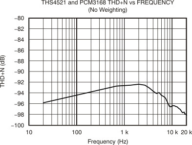 Figure 81. THS4521 and PCM3168: Thd+N Versus Frequency With No Weighting
Table 10. 1-kHz AC Analysis: Test Circuit vs PCM3168 Data Sheet Typical Specifications (FS = 48 kSPS)
| Configuration | Tone | THD+N |
|---|---|---|
| THS4521 and PCM3168 | 1 kHz | –92.6 dBc |
| PCM3168A Data sheet (typ) | 1 kHz | –93 dBc |
9.2.1.3 Application Curves
 Figure 82. THS4521 and PCM4204: Thd+N Versus Frequency With No Weighting
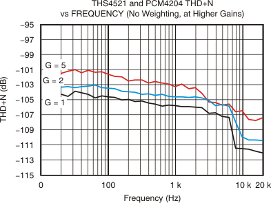 Figure 84. THS4521 and PCM4204: Thd+N Versus Frequency With No Weighting at Higher Gains
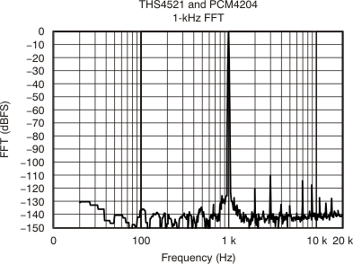 Figure 83. THS4521 and PCM4204 1-kHz FFT
9.2.2 ADC Driver Performance: THS4521 and ADS1278 Combined Performance
The THS4521 provides excellent performance when driving high-performance ΔΣ and successive approximation register (SAR) ADCs in audio and industrial applications using a single 3-V to 5-V power supply. To show achievable performance, the THS4521 is tested as the drive amplifier for the ADS1278 24-bit ADC. The ADS1278 offers excellent ac and DC performance, with four selectable operating
modes from 10 kSPS to 128 kSPS to enable the user to fine-tune performance and power for specific application needs. The circuit shown in Figure 85 was used to test the performance. Data were taken using the High-Resolution mode (52 kSPS) of the ADS1278 with input frequencies at 1 kHz and 10 kHz and signal levels 1/2 dB below full-scale (–0.5 dBFS). FFT plots showing the spectral performance are given in Figure 87 and Figure 88; tabulated ac analysis results are shown in Table 11 and compared to the ADS1278 data sheet typical performance specifications.
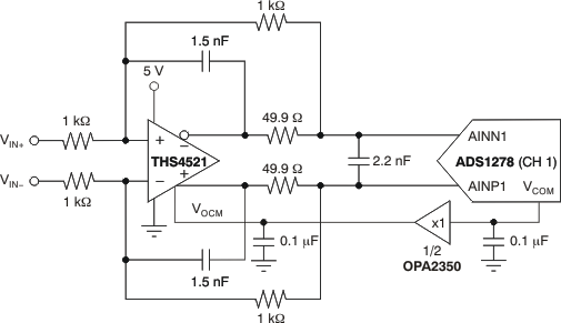 Figure 85. THS4521 and ADS1278 (Ch 1) Test Circuit
9.2.2.1 Design Requirements
Table 11. AC Analysis
| Configuration | Tone | Signal (dBFS) | SNR (dBc) | THD (dBc) | SINAD (dBc) | SFDR (dBc) |
|---|---|---|---|---|---|---|
| THS4521 and ADS1278 | 1 kHz | –0.5 | 109 | –108 | 105 | 114 |
| 10 kHz | –0.5 | 102 | –110 | 101 | 110 | |
| ADS1278 Data sheet (typ) | 1 kHz | –0.5 | 110 | –108 | — | 109 |
9.2.2.2 Detailed Design Procedure
9.2.2.2.1 ADC Driver Performance: THS4521 and ADS8321 Combined Performance
To demonstrate achievable performance, the THS4521 is tested as the drive amplifier for the ADS8321 16-bit SAR ADC. The ADS8321 offers excellent ac and dc performance, with ultra-low power and small size. The circuit shown in Figure 86 was used to test the performance.
Data were taken using the ADS8321 at 100 kSPS with input frequencies of 2 kHz and 10 kHz and signal levels that were -0.5 dBFS. FFT plots that illustrate the spectral performance are given in Figure 89 and Figure 90. Tabulated ac analysis results are listed in Table 12 and compared to the ADS8321 data sheet typical performance. Note the significant improvement in SFD using the THS4521 driver over just the ADC by itself.
 Figure 86. THS4521 and ADS8321 Test Circuit
Table 12. AC Analysis
| Configuration | Tone | Signal (dBFS) | SNR (dBc) | THD (dBc) | SINAD (dBc) | SFDR (dBc) |
|---|---|---|---|---|---|---|
| THS4521 and ADS8321 | 2 kHz | –0.5 | 86.7 | –97.8 | 86.4 | 100.7 |
| 10 kHz | –0.5 | 85.2 | –98.1 | 85.2 | 102.2 | |
| ADS8321 Data sheet (typ) | 10 kHz | –0.5 | 87 | –86 | 84 | 86 |
9.2.2.3 Application Curves
The application curves below apply to the ADS14278 test.
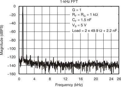 Figure 87. 1-kHz FFT
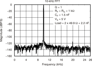 Figure 88. 10-kHz FFT
The application curves below apply to the ADS8321 test.
 Figure 89. 2-kHZ FFT
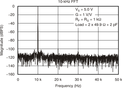 Figure 90. 10-kHz FFT
9.2.3 Differential Input to Differential Output Amplifier
The THS4521, THS4522, and THS4524 family are fully-differential operational amplifiers that can be used to amplify differential input signals to differential output signals. Figure 91 shows a basic block diagram of the circuit (VOCM and PD inputs not shown). The gain of the circuit is set by RF divided by RG.
 Figure 91. Differential Input to Differential Output Amplifier
9.2.4 Single-Ended Input to Differential Output Amplifier
The THS4521, THS4522, and THS4524 family can also amplify and convert single-ended input signals to differential output signals. Figure 92 illustrates a basic block diagram of the circuit (VOCM and PD inputs not shown). The gain of the circuit is again set by RF divided by RG.
 Figure 92. Single-Ended Input to Differential Output Amplifier

