SLOS358C September 2011 – April 2020 THS4531
PRODUCTION DATA.
- 1 Features
- 2 Applications
- 3 Description
- 4 Revision History
- 5 Packaging and Ordering Information
- 6 Electrical Specifications
- 7 Device Information
- 8 Table of Graphs
- 9 Typical Characteristics: VS = 2.7 V
- 10Typical Characteristics: VS = 5 V
-
11Application Information
- 11.1 Typical Characteristics Test Circuits
- 11.2
Application Circuits
- 11.2.1 Differential Input to Differential Output Amplifier
- 11.2.2 Single-Ended Input to Differential Output Amplifier
- 11.2.3 Differential Input to Single-Ended Output Amplifier
- 11.2.4 Input Common-Mode Voltage Range
- 11.2.5 Setting the Output Common-Mode Voltage
- 11.2.6 Single-Supply Operation
- 11.2.7 Low Power Applications and the Effects of Resistor Values on Bandwidth
- 11.2.8 Driving Capacitive Loads
- 11.2.9 Audio Performance
- 11.2.10 Audio On and Off Pop Performance
- 11.3 Audio ADC Driver Performance: THS4531 AND PCM4204 Combined Performance
- 11.4 SAR ADC Performance
- 11.5 EVM and Layout Recommendations
- 12Device and Documentation Support
- 13Mechanical, Packaging, and Orderable Information
封装选项
机械数据 (封装 | 引脚)
散热焊盘机械数据 (封装 | 引脚)
- RUN|10
订购信息
11.2.7 Low Power Applications and the Effects of Resistor Values on Bandwidth
The THS4531 is designed for the nominal value of RF to be 2 kΩ. This gives excellent distortion performance, maximum bandwidth, best flatness, and best pulse response. It also loads the amplifier. For example, in gain of 1 with RF = RG = 2 kΩ, RG to ground, and VOUT+ = 4 V, 1 mA of current will flow through the feedback path to ground. In low power applications, it is desirable to reduce this current by increasing the gain setting resistors values. Using larger value gain resistors has two primary side effects (other than lower power) due to their interaction with the device and PCB parasitic capacitance:
- Lowers the bandwidth.
- Lowers the phase margin
- This will cause peaking in the frequency response.
- And will cause over shoot and ringing in the pulse response.
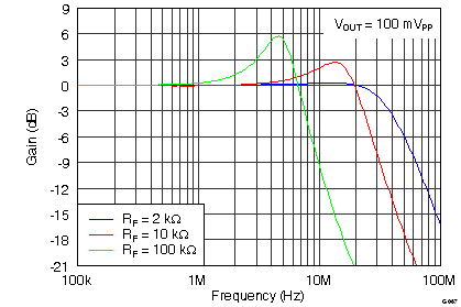
Figure 76 shows the small signal frequency response for gain of 1 with RF and RG equal to 2 kΩ, 10 kΩ, and 100 kΩ. The test was done with RL = 2 kΩ. Due to loading effects of RL, lower values may reduce the peaking, but higher values will not have a significant effect.
As expected, larger value gain resistors cause lower bandwidth and peaking in the response (peaking in frequency response is synonymous with overshoot and ringing in pulse response).
 Figure 76. THS4531 Frequency Response with Various Gain Setting Resistor Values