SLOS358C September 2011 – April 2020 THS4531
PRODUCTION DATA.
- 1 Features
- 2 Applications
- 3 Description
- 4 Revision History
- 5 Packaging and Ordering Information
- 6 Electrical Specifications
- 7 Device Information
- 8 Table of Graphs
- 9 Typical Characteristics: VS = 2.7 V
- 10Typical Characteristics: VS = 5 V
-
11Application Information
- 11.1 Typical Characteristics Test Circuits
- 11.2
Application Circuits
- 11.2.1 Differential Input to Differential Output Amplifier
- 11.2.2 Single-Ended Input to Differential Output Amplifier
- 11.2.3 Differential Input to Single-Ended Output Amplifier
- 11.2.4 Input Common-Mode Voltage Range
- 11.2.5 Setting the Output Common-Mode Voltage
- 11.2.6 Single-Supply Operation
- 11.2.7 Low Power Applications and the Effects of Resistor Values on Bandwidth
- 11.2.8 Driving Capacitive Loads
- 11.2.9 Audio Performance
- 11.2.10 Audio On and Off Pop Performance
- 11.3 Audio ADC Driver Performance: THS4531 AND PCM4204 Combined Performance
- 11.4 SAR ADC Performance
- 11.5 EVM and Layout Recommendations
- 12Device and Documentation Support
- 13Mechanical, Packaging, and Orderable Information
封装选项
机械数据 (封装 | 引脚)
散热焊盘机械数据 (封装 | 引脚)
- RUN|10
订购信息
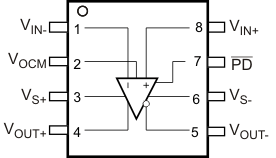
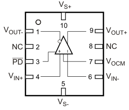
7.1 PIN Configurations
| THS4531 | THS4531 |
|---|---|
| SOIC-8 (D), VSSOP-8 (DGK) PACKAGE (TOP VIEW) | WQFN-10 (RUN) PACKAGE (TOP VIEW) |
 |
 |
Table 2. PIN Functions
| NUMBER | NAME | DESCRIPTION |
|---|---|---|
| THS4531 D, DGK PACKAGE | ||
| 1 | VIN– | Inverted (negative) output feedback |
| 2 | VOCM | Common-mode voltage input |
| 3 | VS+ | Amplifier positive power-supply input |
| 4 | VOUT+ | Non-inverted amplifier output |
| 5 | VOUT– | Inverted amplifier output |
| 6 | VS– | Amplifier negative power-supply input. Note: VS– tied together on multichannel devices. |
| 7 | PD | Power-down, PD = logic low = low power mode, PD = logic high = normal operation (pin must be driven) |
| 8 | VIN+ | Non-inverted amplifier input |
| THS4531 RUN PACKAGE | ||
| 1 | VOUT– | Inverted amplifier output |
| 2, 8 | NC | No internal connection |
| 3 | PD | Power-down, PD = logic low = low power mode, PD = logic high = normal operation (pin must be driven) |
| 4 | VIN+ | Noninverted amplifier input |
| 5 | VS– | Amplifier negative power-supply input. Note: VS– tied together on multichannel devices. |
| 6 | VIN– | Inverting amplifier input |
| 7 | VOCM | Common-mode voltage input |
| 9 | VOUT+ | Noninverted amplifier output |
| 10 | VS+ | Amplifier positive power-supply input |