SLOS358C September 2011 – April 2020 THS4531
PRODUCTION DATA.
- 1 Features
- 2 Applications
- 3 Description
- 4 Revision History
- 5 Packaging and Ordering Information
- 6 Electrical Specifications
- 7 Device Information
- 8 Table of Graphs
- 9 Typical Characteristics: VS = 2.7 V
- 10Typical Characteristics: VS = 5 V
-
11Application Information
- 11.1 Typical Characteristics Test Circuits
- 11.2
Application Circuits
- 11.2.1 Differential Input to Differential Output Amplifier
- 11.2.2 Single-Ended Input to Differential Output Amplifier
- 11.2.3 Differential Input to Single-Ended Output Amplifier
- 11.2.4 Input Common-Mode Voltage Range
- 11.2.5 Setting the Output Common-Mode Voltage
- 11.2.6 Single-Supply Operation
- 11.2.7 Low Power Applications and the Effects of Resistor Values on Bandwidth
- 11.2.8 Driving Capacitive Loads
- 11.2.9 Audio Performance
- 11.2.10 Audio On and Off Pop Performance
- 11.3 Audio ADC Driver Performance: THS4531 AND PCM4204 Combined Performance
- 11.4 SAR ADC Performance
- 11.5 EVM and Layout Recommendations
- 12Device and Documentation Support
- 13Mechanical, Packaging, and Orderable Information
封装选项
机械数据 (封装 | 引脚)
散热焊盘机械数据 (封装 | 引脚)
- RUN|10
订购信息
11.2.5 Setting the Output Common-Mode Voltage
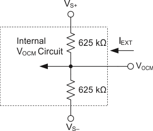
The output common-model voltage is set by the voltage at the VOCM pin and the internal circuit works to maintain the output common-mode voltage as close as possible to this voltage. If left unconnected, the output common-mode is set to mid-supply by internal circuitry, which may be over-driven from an external source. Figure 75 is representative of the VOCM input. The internal VOCM circuit has about 24 MHz of -3 dB bandwidth, which is required for best performance, but it is intended to be a DC bias input pin. Bypass capacitors are recommended on this pin to reduce noise. The external current required to overdrive the internal resistor divider is given approximately by the formula:

where VOCM is the voltage applied to the VOCM pin.
 Figure 75. Simplified VOCM Input Circuit