SLOS358C September 2011 – April 2020 THS4531
PRODUCTION DATA.
- 1 Features
- 2 Applications
- 3 Description
- 4 Revision History
- 5 Packaging and Ordering Information
- 6 Electrical Specifications
- 7 Device Information
- 8 Table of Graphs
- 9 Typical Characteristics: VS = 2.7 V
- 10Typical Characteristics: VS = 5 V
-
11Application Information
- 11.1 Typical Characteristics Test Circuits
- 11.2
Application Circuits
- 11.2.1 Differential Input to Differential Output Amplifier
- 11.2.2 Single-Ended Input to Differential Output Amplifier
- 11.2.3 Differential Input to Single-Ended Output Amplifier
- 11.2.4 Input Common-Mode Voltage Range
- 11.2.5 Setting the Output Common-Mode Voltage
- 11.2.6 Single-Supply Operation
- 11.2.7 Low Power Applications and the Effects of Resistor Values on Bandwidth
- 11.2.8 Driving Capacitive Loads
- 11.2.9 Audio Performance
- 11.2.10 Audio On and Off Pop Performance
- 11.3 Audio ADC Driver Performance: THS4531 AND PCM4204 Combined Performance
- 11.4 SAR ADC Performance
- 11.5 EVM and Layout Recommendations
- 12Device and Documentation Support
- 13Mechanical, Packaging, and Orderable Information
封装选项
机械数据 (封装 | 引脚)
散热焊盘机械数据 (封装 | 引脚)
- RUN|10
订购信息
10 Typical Characteristics: VS = 5 V
Test conditions unless otherwise noted: VS+ = 5 V, VS– = 0 V, VOCM = open, VOUT = 2 Vpp, RF = 2 kΩ, RL = 2 kΩ Differential, G = 1 V/V, Single-Ended Input, Differential Output, Input and Output Referenced to mid-supply, TA = 25°C unless otherwise noted.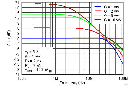 Figure 34. Small-Signal Frequency Response
 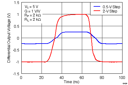 Figure 36. Large and Small-Signal Pulse Response
 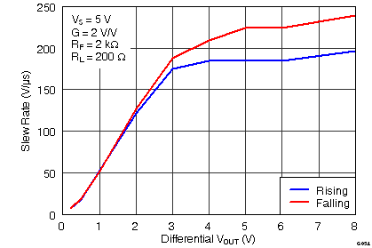 Figure 38. Differential Slew Rate vs VOUT Step
  Figure 40. 10 kHz FFT On Audio Analyzer
  Figure 42. Harmonic Distortion vs Output Voltage at 1 MHz
 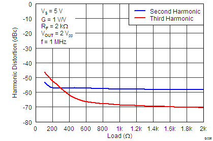 Figure 44. Harmonic Distortion vs Load at 1 MHz
  Figure 46. Two-Tone, 2nd and 3rdOrder Intermodulation Distortion vs Frequency
  Figure 48. Single-Ended Output Saturation Voltage vs Load Current
 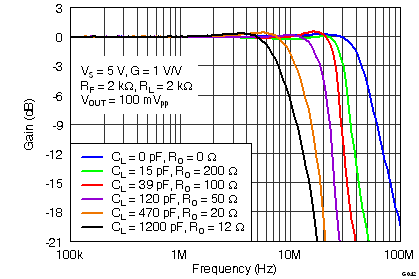 Figure 50. Frequency Response vs CLOAD
 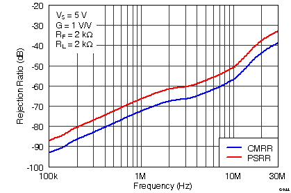 Figure 52. Rejection Ratio vs Frequency
 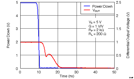 Figure 54. Turn-Off Time
 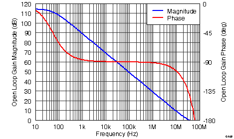 Figure 56. Main Amplifier Differential Open-Loop Gain and Phase vs Frequency
 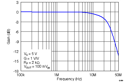 Figure 58. VOCM Small-Signal Frequency Response
 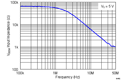 Figure 60. VOCM Input Impedance vs Frequency
 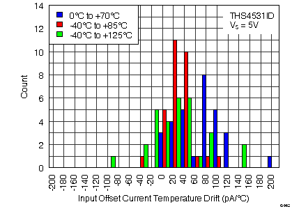 Figure 62. Input Offset Current Temperature Drift Histogram
 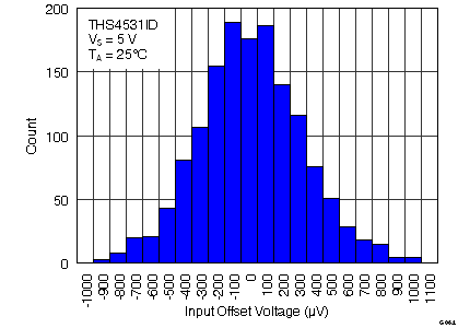 Figure 64. Input Offset Voltage Histogram
 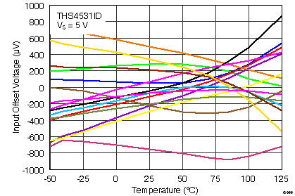 Figure 66. Input Offset Voltage vs Temperature
 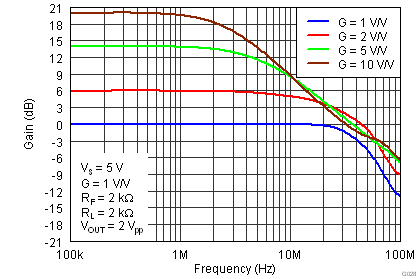 Figure 35. Large-Signal Frequency Response
 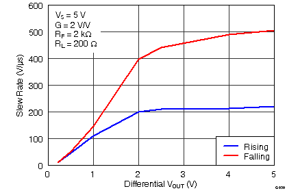 Figure 37. Single-Ended Slew Rate vs VOUT Step
 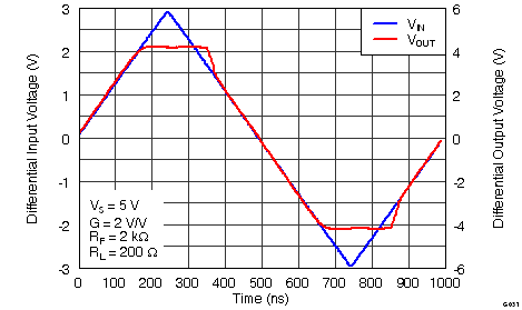 Figure 39. Overdrive Recovery
 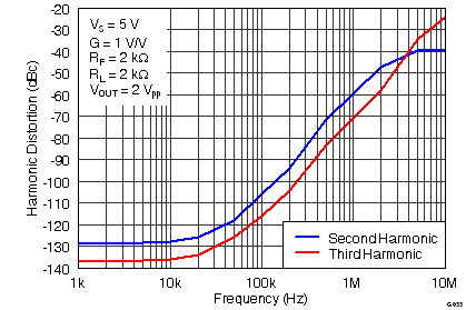 Figure 41. Harmonic Distortion vs Frequency
 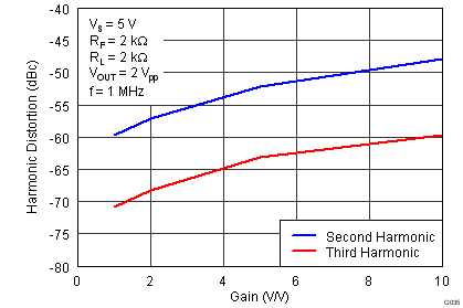 Figure 43. Harmonic Distortion vs Gain at 1 MHz
 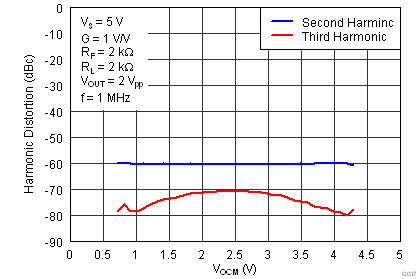 Figure 45. Harmonic Distortion vs VOCM at 1 MHz
  Figure 47. Single-Ended Output Voltage Swing vs Load Resistance
 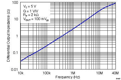 Figure 49. Main Amplifier Differential Output Impedance vs Frequency
 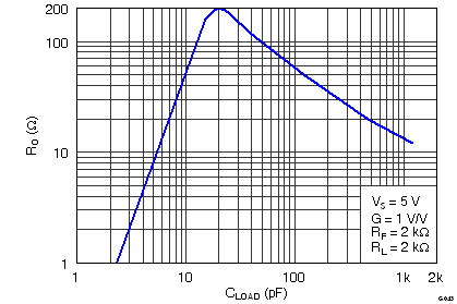 Figure 51. RO vs CLOAD
 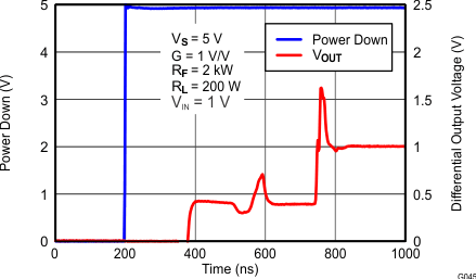 Figure 53. Turn-On Time
  Figure 55. Input-Referred Voltage Noise and Current Noise Spectral Density
 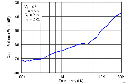 Figure 57. Output Balance Error vs Frequency
 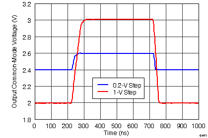 Figure 59. VOCM Large and Small-Signal Pulse Response
 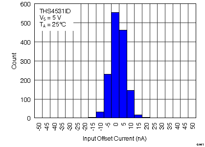 Figure 61. Input Offset Current Histogram
 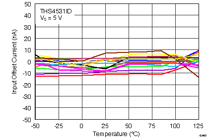 Figure 63. Input Offset Current vs Temperature
 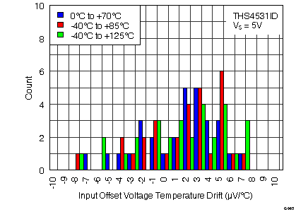 Figure 65. Input Offset Voltage Temperature Drift Histogram