ZHCSFB6D April   2016  – June 2021 THS4551

PRODUCTION DATA  

  1. 特性
  2. 应用
  3. 描述
  4. Revision History
  5. Companion Devices
  6. Pin Configuration and Functions
  7. Specifications
    1. 7.1 Absolute Maximum Ratings
    2. 7.2 ESD Ratings
    3. 7.3 Recommended Operating Conditions
    4. 7.4 Thermal Information
    5. 7.5 Electrical Characteristics: (VS+) – (VS–) = 5 V
    6. 7.6 Electrical Characteristics: (VS+) – (VS–) = 3 V
    7. 7.7 Typical Characteristics: (VS+) – (VS–) = 5 V
    8. 7.8 Typical Characteristics: (VS+) – (VS–) = 3 V
    9. 7.9 Typical Characteristics: 3-V to 5-V Supply Range
  8. Parameter Measurement Information
    1. 8.1 Example Characterization Circuits
    2. 8.2 Output Interface Circuit for DC-Coupled Differential Testing
    3. 8.3 Output Common-Mode Measurements
    4. 8.4 Differential Amplifier Noise Measurements
    5. 8.5 Balanced Split-Supply Versus Single-Supply Characterization
    6. 8.6 Simulated Characterization Curves
    7. 8.7 Terminology and Application Assumptions
  9. Detailed Description
    1. 9.1 Overview
    2. 9.2 Functional Block Diagram
    3. 9.3 Feature Description
      1. 9.3.1 Differential Open-Loop Gain and Output Impedance
      2. 9.3.2 Setting Resistor Values Versus Gain
      3. 9.3.3 I/O Headroom Considerations
      4. 9.3.4 Output DC Error and Drift Calculations and the Effect of Resistor Imbalances
    4. 9.4 Device Functional Modes
      1. 9.4.1 Operation from Single-Ended Sources to Differential Outputs
        1. 9.4.1.1 AC-Coupled Signal Path Considerations for Single-Ended Input to Differential Output Conversions
        2. 9.4.1.2 DC-Coupled Input Signal Path Considerations for Single-Ended to Differential Conversions
      2. 9.4.2 Operation from a Differential Input to a Differential Output
        1. 9.4.2.1 AC-Coupled, Differential-Input to Differential-Output Design Issues
        2. 9.4.2.2 DC-Coupled, Differential-Input to Differential-Output Design Issues
      3. 9.4.3 Input Overdrive Performance
  10. 10Application and Implementation
    1. 10.1 Application Information
      1. 10.1.1 Noise Analysis
      2. 10.1.2 Factors Influencing Harmonic Distortion
      3. 10.1.3 Driving Capacitive Loads
      4. 10.1.4 Interfacing to High-Performance Precision ADCs
      5. 10.1.5 Operating the Power Shutdown Feature
      6. 10.1.6 Designing Attenuators
      7. 10.1.7 The Effect of Adding a Feedback Capacitor
    2. 10.2 Typical Applications
      1. 10.2.1 An MFB Filter Driving an ADC Application
        1. 10.2.1.1 Design Requirements
        2. 10.2.1.2 Detailed Design Procedure
        3. 10.2.1.3 Application Curves
      2. 10.2.2 Differential Transimpedance Output to a High-Grade Audio PCM DAC Application
        1. 10.2.2.1 Design Requirements
        2. 10.2.2.2 Detailed Design Procedure
        3. 10.2.2.3 Application Curves
      3. 10.2.3 ADC3k Driver with a 2nd-Order RLC Interstage Filter Application
        1. 10.2.3.1 Design Requirements
        2. 10.2.3.2 Detailed Design Procedure
        3. 10.2.3.3 Application Curve
  11. 11Power Supply Recommendations
    1. 11.1 Thermal Analysis
  12. 12Layout
    1. 12.1 Layout Guidelines
      1. 12.1.1 Board Layout Recommendations
    2. 12.2 Layout Example
    3. 12.3 EVM Board
  13. 13Device and Documentation Support
    1. 13.1 Device Support
      1. 13.1.1 TINA-TI Simulation Model Features
    2. 13.2 Documentation Support
      1. 13.2.1 Related Documentation
    3. 13.3 接收文档更新通知
    4. 13.4 支持资源
    5. 13.5 Trademarks
    6. 13.6 静电放电警告
    7. 13.7 术语表
  14. 14Mechanical, Packaging, and Orderable Information

封装选项

机械数据 (封装 | 引脚)
散热焊盘机械数据 (封装 | 引脚)
订购信息

Output Common-Mode Measurements

The circuit of Figure 8-5 is a typical setup for common-mode measurements.
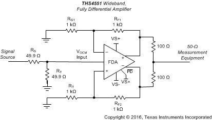
GUID-A84D914E-BA26-4AFF-93FE-58E756114629-low.gif Figure 8-5 Output Common-Mode Measurements

In Figure 8-5, the differential path is simply terminated back to ground on the two 1-kΩ input resistors and the VOCM control input is driven from a 50-Ω matched source for the frequency response and step response curves of Figure 7-43 and Figure 7-44. The outputs are summed to a center point (to obtain the average, or common-mode, output) through two 100-Ω resistors. These 100-Ω resistors form an equivalent 50-Ω source to the common-mode output for measurements. This common-mode test circuit is available as a TINA-TI™ simulation file. Figure 7-45 illustrates the common-mode output noise measurements with either a ground on the VOCM input pin or with the VOCM input pin floating. The higher noise in Figure 7-45 for a floated input can be reduced by including a capacitor to ground at the VOCM control input pin.