ZHCSFB6D April 2016 – June 2021 THS4551
PRODUCTION DATA
- 1 特性
- 2 应用
- 3 描述
- 4 Revision History
- 5 Companion Devices
- 6 Pin Configuration and Functions
-
7 Specifications
- 7.1 Absolute Maximum Ratings
- 7.2 ESD Ratings
- 7.3 Recommended Operating Conditions
- 7.4 Thermal Information
- 7.5 Electrical Characteristics: (VS+) – (VS–) = 5 V
- 7.6 Electrical Characteristics: (VS+) – (VS–) = 3 V
- 7.7 Typical Characteristics: (VS+) – (VS–) = 5 V
- 7.8 Typical Characteristics: (VS+) – (VS–) = 3 V
- 7.9 Typical Characteristics: 3-V to 5-V Supply Range
-
8 Parameter Measurement Information
- 8.1 Example Characterization Circuits
- 8.2 Output Interface Circuit for DC-Coupled Differential Testing
- 8.3 Output Common-Mode Measurements
- 8.4 Differential Amplifier Noise Measurements
- 8.5 Balanced Split-Supply Versus Single-Supply Characterization
- 8.6 Simulated Characterization Curves
- 8.7 Terminology and Application Assumptions
- 9 Detailed Description
- 10Application and Implementation
- 11Power Supply Recommendations
- 12Layout
- 13Device and Documentation Support
- 14Mechanical, Packaging, and Orderable Information
封装选项
机械数据 (封装 | 引脚)
散热焊盘机械数据 (封装 | 引脚)
订购信息
9.4.2.2 DC-Coupled, Differential-Input to Differential-Output Design Issues
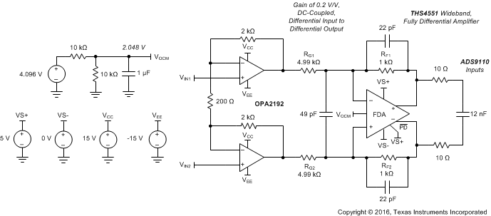
Operating the THS4551 with a dc-coupled differential input source is very simple and only requires that the input pins stay in range for the dc common-mode operating voltage. The example in Figure 9-11 takes the output of a dual precision op amp (such as the OPA2192) where a high differential input signal is attenuated by the THS4551 down into the range of an 18-bit SAR ADC such as the 2-MSPS ADS9110. The input stage provides a differential gain of 21 V/V with a common-mode gain of 1 V/V. This example amplifies a small differential signal on top of a very-wide range common-mode voltage. The input common-mode voltage appears at the outputs of the OPA2192. The input common-mode voltage is level shifted by the FDA common-mode control to be at the required output common-mode voltage to drive the ADS9110 SAR ADC (with a 4.096-V reference, as shown in Figure 9-11); the FDA output common-mode voltage must be at the 2.048 V shown in Figure 9-11. This design offers a very high CMRR using the common-mode control loop of the FDA to reset the output common-mode voltage from that delivered to the inputs of the OPA2192. The actual CMRR from the OPA2192 inputs to the FDA outputs is dominated by the resistor mismatches in the FDA. The feedback and differential input capacitors are included to shape the noise gain as described in Section 10.1.6. This full example circuit is available as a TINA-TI™ simulation file.
 Figure 9-11 Example
DC-Coupled Differential I/O Design from a Precision Dual Op Amp to an 18-Bit
SAR