ZHCSFB6D April 2016 – June 2021 THS4551
PRODUCTION DATA
- 1 特性
- 2 应用
- 3 描述
- 4 Revision History
- 5 Companion Devices
- 6 Pin Configuration and Functions
-
7 Specifications
- 7.1 Absolute Maximum Ratings
- 7.2 ESD Ratings
- 7.3 Recommended Operating Conditions
- 7.4 Thermal Information
- 7.5 Electrical Characteristics: (VS+) – (VS–) = 5 V
- 7.6 Electrical Characteristics: (VS+) – (VS–) = 3 V
- 7.7 Typical Characteristics: (VS+) – (VS–) = 5 V
- 7.8 Typical Characteristics: (VS+) – (VS–) = 3 V
- 7.9 Typical Characteristics: 3-V to 5-V Supply Range
-
8 Parameter Measurement Information
- 8.1 Example Characterization Circuits
- 8.2 Output Interface Circuit for DC-Coupled Differential Testing
- 8.3 Output Common-Mode Measurements
- 8.4 Differential Amplifier Noise Measurements
- 8.5 Balanced Split-Supply Versus Single-Supply Characterization
- 8.6 Simulated Characterization Curves
- 8.7 Terminology and Application Assumptions
- 9 Detailed Description
- 10Application and Implementation
- 11Power Supply Recommendations
- 12Layout
- 13Device and Documentation Support
- 14Mechanical, Packaging, and Orderable Information
封装选项
机械数据 (封装 | 引脚)
散热焊盘机械数据 (封装 | 引脚)
订购信息
10.1.7 The Effect of Adding a Feedback Capacitor
Adding a feedback capacitor to band-limit the signal path is very common in lower frequency designs. This approach is very effective for the signal path gain but does create the potential for high-frequency peaking and oscillation for a wideband device such as the THS4551. The feedback capacitor by itself takes the noise gain to 1 V/V at high frequencies. Depending on the frequency where the noise gain goes to 1V/V, and what added phase margin reduction may already be in place resulting from the load RC, the feedback capacitors can cause instability.
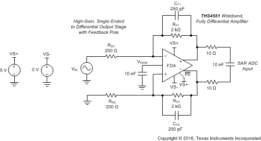
Figure 10-7 shows the starting point for a typical band-limited design. At lower frequencies, this example delivers a gain of 10 V/V with an intentional band limit in the feedback RC at 320 kHz. This single 5-V design targets a midsupply output common-mode voltage with only a noise reduction capacitor on the VOCM input control.
 Figure 10-7 Single-Ended to Differential Stage with a Feedback Pole
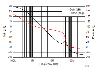
The response shape must be probed at the FDA output pins before the added RC pole to the SAR input. Running a wideband sweep with the THS4551 TINA-TI™ model using the SBOC475 simulation file shows a resonance at 50 MHz in Figure 10-8 resulting from the feedback capacitor.
 Figure 10-8 Gain and Phase Plot with a Feedback Pole
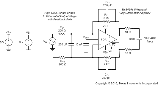
One approach to increasing the phase margin when there is a feedback capacitor is to include a differential input capacitor. This approach increases the noise gain at higher frequencies, thus creating a lower-frequency loop gain equal to a 0-dB crossover with more phase margin. Figure 10-9 shows a differential input capacitor equal to the feedback capacitor in the test circuit. This approach increases the noise gain from 1 V/V at higher frequencies (with only a feedback capacitor) to a noise gain of 3 V/V at higher frequencies.
 Figure 10-9 Single-Ended to Differential Stage with a Feedback Pole and Differential Input Capacitor
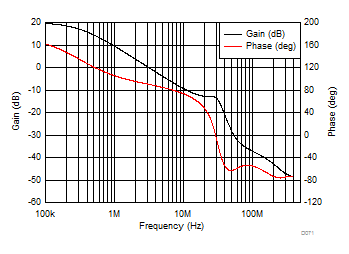
Re-running the wideband response (using the SBOC474 TINA-TI™ simulation file) simulation illustrates in Figure 10-10 that the resonance is greatly reduced with the higher noise gain at the loop gain equal to a 0-dB crossover at a lower frequency. Although this example is only modestly peaking, good design practice is to include a place for a differential input capacitor (even if not used) for any design using a feedback capacitor across the feedback resistors. This recommendation applies to this simple example and to multiple feedback active filter designs.
 Figure 10-10 Gain and Phase Plot with a Differential Input Capacitor