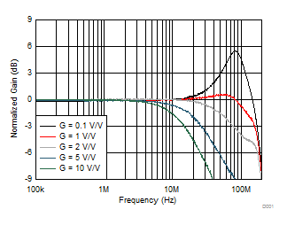
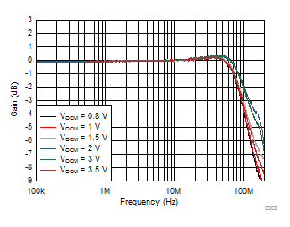
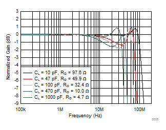
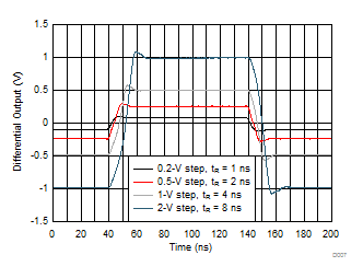
at TA ≈ 25°C, VOCM pin = open, RF = 1 kΩ, RL = 1 kΩ, VOUT = 2 VPP, 50-Ω input match, G = 1 V/V,
PD = VS+, single-ended input, differential output, and input and output referenced to default midsupply for ac-coupled tests (unless otherwise noted); see Figure 8-1 for a gain of 1-V/V test circuit
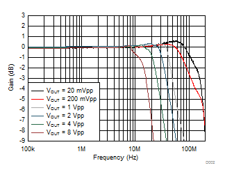
 Figure 7-1 Small-Signal Frequency Response vs Gain
| VOUT = 20 mVPP , see Figure 8-1 with VOCM adjusted |
Figure 7-3 Small-Signal Frequency Response vs VOCM
| VOUT = 20 mVPP at load, G =
1, two series RO added at output before
capacitive load (CL) |
Figure 7-5 Small-Signal Frequency Response vs CL
| G =
1 V/V, 5-MHz input, single-ended to differential
output |
Figure 7-7 Small- and Large-Signal Step Response
| G =
2 V/V, 5-MHz input, single-ended input to differential
output |
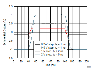
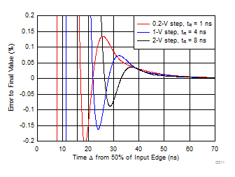
Figure 7-9 Small- and Large-Signal Step Response Figure 7-11 Small- and Large-Signal Step Settling Time
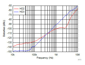
 Figure 7-13 Harmonic Distortion vs Frequency
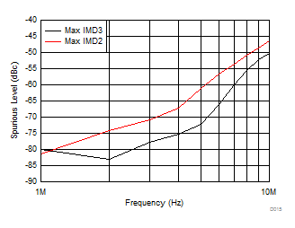
| G =
1 V/V, VOUT = 1 VPP each
tone |
Figure 7-15 Intermodulation Distortion (IMD2 and IMD3) vs Frequency
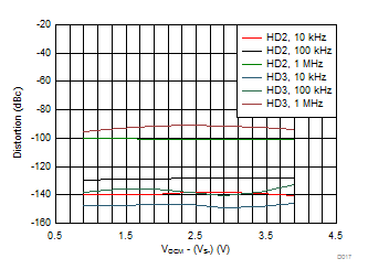
| G =
1 V/V, VOUT = 2 VPP, with
VOCM adjusted |
Figure 7-17 Harmonic Distortion vs VOCM Figure 7-2 Frequency Response vs VOUT
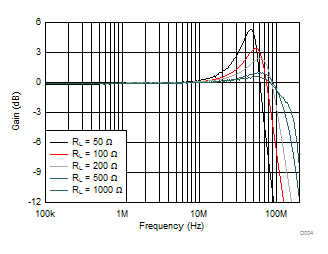
| VOUT = 20 mVPP, see Figure 8-1 with load resistance (RL) adjusted |
Figure 7-4 Small-Signal Frequency Response vs RL
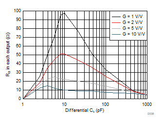
| Output resistance (RO) is two series output
resistors to a differential CL in parallel
with a 1-kΩ load resistance |
Figure 7-6 Recommended RO vs CL
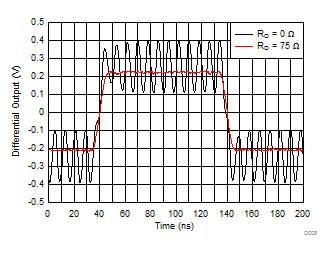
| G =
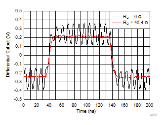
1 V/V, VOUT = 500-mV step into 22-pF
CL, see Figure 8-4 |
Figure 7-8 Step
Response Into Capacitive Load
| G =
2 V/V, VOUT = 500-mV step into 22-pF
CL, see Figure 8-4 |
Figure 7-10 Step
Response Into Capacitive Load
| Single-ended to differential gain of 2, 2X input
overdrive |
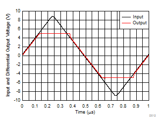
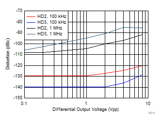
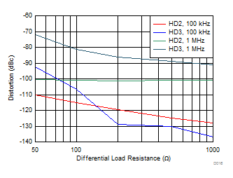
Figure 7-12 Overdrive Recovery Performance Figure 7-14 Harmonic Distortion vs Output Swing
| G =
1 V/V, VOUT = 2 VPP, with
RL adjusted |
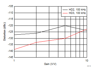
Figure 7-16 Harmonic Distortion vs RL Figure 7-18 Harmonic Distortion vs Gain