ZHCSFB6D April 2016 – June 2021 THS4551
PRODUCTION DATA
- 1 特性
- 2 应用
- 3 描述
- 4 Revision History
- 5 Companion Devices
- 6 Pin Configuration and Functions
-
7 Specifications
- 7.1 Absolute Maximum Ratings
- 7.2 ESD Ratings
- 7.3 Recommended Operating Conditions
- 7.4 Thermal Information
- 7.5 Electrical Characteristics: (VS+) – (VS–) = 5 V
- 7.6 Electrical Characteristics: (VS+) – (VS–) = 3 V
- 7.7 Typical Characteristics: (VS+) – (VS–) = 5 V
- 7.8 Typical Characteristics: (VS+) – (VS–) = 3 V
- 7.9 Typical Characteristics: 3-V to 5-V Supply Range
-
8 Parameter Measurement Information
- 8.1 Example Characterization Circuits
- 8.2 Output Interface Circuit for DC-Coupled Differential Testing
- 8.3 Output Common-Mode Measurements
- 8.4 Differential Amplifier Noise Measurements
- 8.5 Balanced Split-Supply Versus Single-Supply Characterization
- 8.6 Simulated Characterization Curves
- 8.7 Terminology and Application Assumptions
- 9 Detailed Description
- 10Application and Implementation
- 11Power Supply Recommendations
- 12Layout
- 13Device and Documentation Support
- 14Mechanical, Packaging, and Orderable Information
封装选项
机械数据 (封装 | 引脚)
散热焊盘机械数据 (封装 | 引脚)
订购信息
11 Power Supply Recommendations
The THS4551 is principally intended to operate with a nominal single-supply voltage of 3 V to 5 V. Supply voltage tolerances are supported with the specified operating range of 2.7 V (10% low on a 3-V nominal supply) and 5.4 V (8% high on a 5-V nominal supply). Supply decoupling is required, as described in Section 8.7. Split (or bipolar) supplies can be used with the THS4551, as long as the total value across the device remains less than 5.5 V (absolute maximum). The thermal pad on the RGT package is electrically isolated form the die; connect the thermal pad (RGT package only) to any power or ground plane for reduced thermal impedance to the junction temperature. This pad must be connected to some power or ground plane and not floated.
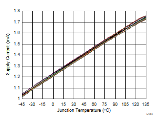
For the best input offset voltage drift, the THS4551 uses a proportional to absolute temperature (PTAT) quiescent current biasing scheme. This approach gives a positive over temperature variation in supply current. Figure 11-1 shows the 5-V supply current over a wide TJ range for a number of tested units. The Electrical Characteristics tables report the typical and range on this supply current temperature coefficient for both 5-V and 3-V supply operation.
 Figure 11-1 Linear Temperature Coefficient for Supply
Current
Figure 11-1 Linear Temperature Coefficient for Supply
CurrentUsing a negative supply to deliver a true swing to ground output when driving SAR ADCs can be desired. Although the THS4551 quotes a rail-to-rail output, linear operation requires approximately 200-mV headroom to the supply rails. One easy option for extending the linear output swing to ground is to provide the small negative supply voltage required using the LM7705 fixed –230-mV, negative-supply generator. This low-cost, fixed, negative-supply generator can accept the 3-V to 5-V positive supply input used by the THS4551 and provides a fixed –230-mV supply for the negative power supply. Using the LM7705 provides an effective solution, as discussed in the Extending Rail-to-Rail Output Range for Fully Differential Amplifiers to Include True Zero Volts TI design (TIDU187)