ZHCSFB6D April 2016 – June 2021 THS4551
PRODUCTION DATA
- 1 特性
- 2 应用
- 3 描述
- 4 Revision History
- 5 Companion Devices
- 6 Pin Configuration and Functions
-
7 Specifications
- 7.1 Absolute Maximum Ratings
- 7.2 ESD Ratings
- 7.3 Recommended Operating Conditions
- 7.4 Thermal Information
- 7.5 Electrical Characteristics: (VS+) – (VS–) = 5 V
- 7.6 Electrical Characteristics: (VS+) – (VS–) = 3 V
- 7.7 Typical Characteristics: (VS+) – (VS–) = 5 V
- 7.8 Typical Characteristics: (VS+) – (VS–) = 3 V
- 7.9 Typical Characteristics: 3-V to 5-V Supply Range
-
8 Parameter Measurement Information
- 8.1 Example Characterization Circuits
- 8.2 Output Interface Circuit for DC-Coupled Differential Testing
- 8.3 Output Common-Mode Measurements
- 8.4 Differential Amplifier Noise Measurements
- 8.5 Balanced Split-Supply Versus Single-Supply Characterization
- 8.6 Simulated Characterization Curves
- 8.7 Terminology and Application Assumptions
- 9 Detailed Description
- 10Application and Implementation
- 11Power Supply Recommendations
- 12Layout
- 13Device and Documentation Support
- 14Mechanical, Packaging, and Orderable Information
封装选项
机械数据 (封装 | 引脚)
散热焊盘机械数据 (封装 | 引脚)
订购信息
10.2.2.3 Application Curves
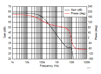
The bandwidth is controlled to 88 kHz by using the 2.4-nF feedback capacitors. Amplifier stability is controlled by the 20-nF differential capacitor across the DAC outputs. The added 4.4 Ω in series with the feedback 2.2-nF capacitor isolates this capacitance from the inductive open-loop output impedance. To observe the effect of adding these small resistors in series with the feedback capacitors, use the TINA-TI™ loop gain simulation circuit. Include the DAC source capacitance in any final design analysis. Running the frequency response for this circuit (available as a TINA-TI™ simulation file) provides this result. The 63.5-dBΩ gain is the 1.5-kΩ transimpedance gain provided in this design.
 Figure 10-15 Gain and Phase Plot of DAC Output Driver
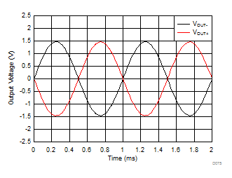
Running a full-scale sine wave at 1 kHz with ±1.95 mA on each output from the DAC at 180° out of phase, and probing each THS4551 output pin separately results in the expected ±1.46 V on each output pin, as shown in Figure 10-16. More output swing is available for the RRO device using the ±2.5-V supplies provided by the LM27762 by simply increasing the feedback resistor values.
 Figure 10-16 Output Waveform of the DAC Output Driver
Although this example is on the audio signal generation side, the THS4551 can also be used to convert a single-ended line input to a differential driver into an audio ADC.