ZHCSI82E May 2018 – May 2019 THVD1410 , THVD1450 , THVD1451 , THVD1452
PRODUCTION DATA.
- 1 特性
- 2 应用
- 3 说明
- 4 修订历史记录
- 5 Device Comparison Table
- 6 Pin Configuration and Functions
-
7 Specifications
- 7.1 Absolute Maximum Ratings
- 7.2 ESD Ratings
- 7.3 ESD Ratings [IEC]
- 7.4 Recommended Operating Conditions
- 7.5 Thermal Information
- 7.6 Power Dissipation
- 7.7 Electrical Characteristics
- 7.8 Switching Characteristics
- 7.9 Typical Characteristics: All Devices
- 7.10 Typical Characteristics: THD1450, THVD1451 and THVD1452
- 7.11 Typical Characteristics: THVD1410
- 8 Parameter Measurement Information
- 9 Detailed Description
- 10Application and Implementation
- 11Power Supply Recommendations
- 12Layout
- 13器件和文档支持
- 14机械、封装和可订购信息
封装选项
请参考 PDF 数据表获取器件具体的封装图。
机械数据 (封装 | 引脚)
- D|8
- DRB|8
散热焊盘机械数据 (封装 | 引脚)
- DRB|8
订购信息
8 Parameter Measurement Information
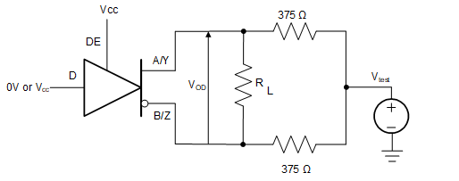
 Figure 21. Measurement of Driver Differential and Common-Mode Output With RS-485 Load
  Figure 22. Measurement of Driver Differential Output Rise and Fall Times and Propagation Delays
  Figure 23. Measurement of Driver Enable and Disable Times With Active High Output and Pull-Down Load
  Figure 24. Measurement of Driver Enable and Disable Times With Active Low Output and Pull-up Load
  Figure 25. Measurement of Receiver Output Rise and Fall Times and Propagation Delays
  Figure 26. Measurement of Receiver Enable/Disable Times With Driver Enabled
  Figure 27. Measurement of Receiver Enable Times With Driver Disabled