ZHCSKF1 October   2019 THVD1520

PRODUCTION DATA.  

  1. 特性
  2. 应用
  3. 说明
    1.     Device Images
      1.      简化原理图
  4. 修订历史记录
  5. Pin Configuration and Functions
    1.     Pin Functions
  6. Specifications
    1. 6.1 Absolute Maximum Ratings
    2. 6.2 ESD Ratings
    3. 6.3 ESD Ratings [IEC]
    4. 6.4 Recommended Operating Conditions
    5. 6.5 Thermal Information
    6. 6.6 Electrical Characteristics
    7. 6.7 Power Dissipation Characteristics
    8. 6.8 Switching Characteristics
    9. 6.9 Typical Characteristics
  7. Parameter Measurement Information
  8. Detailed Description
    1. 8.1 Overview
    2. 8.2 Functional Block Diagrams
    3. 8.3 Feature Description
    4. 8.4 Device Functional Modes
  9. Application and Implementation
    1. 9.1 Application Information
    2. 9.2 Typical Application
      1. 9.2.1 Design Requirements
        1. 9.2.1.1 Data Rate and Bus Length
        2. 9.2.1.2 Stub Length
        3. 9.2.1.3 Bus Loading
        4. 9.2.1.4 Receiver Failsafe
        5. 9.2.1.5 Transient Protection
      2. 9.2.2 Detailed Design Procedure
      3. 9.2.3 Application Curves
  10. 10Power Supply Recommendations
  11. 11Layout
    1. 11.1 Layout Guidelines
    2. 11.2 Layout Example
  12. 12器件和文档支持
    1. 12.1 器件支持
    2. 12.2 第三方米6体育平台手机版_好二三四免责声明
    3. 12.3 接收文档更新通知
    4. 12.4 社区资源
    5. 12.5 商标
    6. 12.6 静电放电警告
    7. 12.7 Glossary
  13. 13机械、封装和可订购信息

封装选项

机械数据 (封装 | 引脚)
散热焊盘机械数据 (封装 | 引脚)
订购信息

Typical Characteristics

VCC = 5 V, TA = 250C (unless otherwise noted)
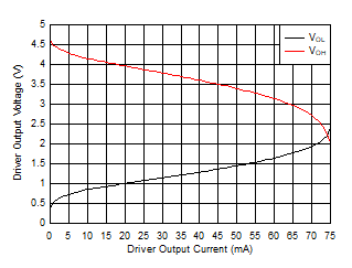
THVD1520 D_001.gifFigure 1. Driver Output Voltage vs Driver Output Current
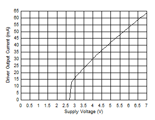
THVD1520 D_003.gifFigure 3. Driver Output Current vs Supply Voltage
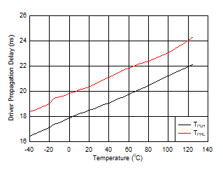
THVD1520 D005.gifFigure 5. Driver Propagation Delay vs Temperature
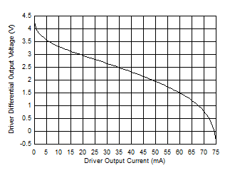
THVD1520 D_002.gifFigure 2. Driver Differential Output Voltage vs Driver Output Current
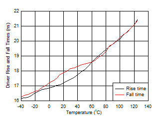
THVD1520 D004.gifFigure 4. Driver Rise or Fall Time vs Temperature
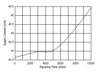
THVD1520 D006.gif
50% duty cycle square-wave RL = 54 Ω CL = 50 pF DE = VCC, RE = GND
Figure 6. Supply Current vs Signaling Rate