ZHCSGQ0A September 2017 – February 2022 TIC10024-Q1
PRODUCTION DATA
- 1 特性
- 2 应用
- 3 说明
- 4 Revision History
- 5 Pin Configuration and Functions
- 6 Specifications
- 7 Parameter Measurement Information
-
8 Detailed Description
- 8.1 Overview
- 8.2 Functional Block Diagram
- 8.3
Feature Description
- 8.3.1 VS Pin
- 8.3.2 VDD Pin
- 8.3.3 Device Initialization
- 8.3.4 Device Trigger
- 8.3.5 Device Reset
- 8.3.6 VS Under-Voltage (UV) Condition
- 8.3.7 VS Over-Voltage (OV) Condition
- 8.3.8 Switch Inputs Settings
- 8.3.9 Interrupt Generation and INT Assertion
- 8.3.10 Temperature Monitor
- 8.3.11 Parity Check And Parity Generation
- 8.3.12 Cyclic Redundancy Check (CRC)
- 8.4 Device Functional Modes
- 9 Programming
- 10Application and Implementation
- 11Power Supply Recommendations
- 12Layout
- 13Device and Documentation Support
- 14Mechanical, Packaging, and Orderable Information
5 Pin Configuration and Functions
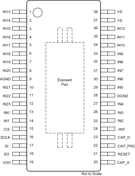
 Figure 5-1 DCP (TSSOP) Package, 38-Pin, Top View
Table 5-1 Pin Functions
| PIN | TYPE(1) | DESCRIPTION | |
|---|---|---|---|
| NO. | NAME | ||
| 1 | IN13 | I/O | Ground switch monitoring input with current source |
| 2 | IN14 | I/O | Ground switch monitoring input with current source |
| 3 | IN15 | I/O | Ground switch monitoring input with current source |
| 4 | IN16 | I/O | Ground switch monitoring input with current source |
| 5 | IN17 | I/O | Ground switch monitoring input with current source |
| 6 | IN18 | I/O | Ground switch monitoring input with current source |
| 7 | IN19 | I/O | Ground switch monitoring input with current source |
| 8 | IN20 | I/O | Ground switch monitoring input with current source |
| 9 | AGND | P | Ground for analog circuitry |
| 10 | IN21 | I/O | Ground switch monitoring input with current source |
| 11 | IN22 | I/O | Ground switch monitoring input with current source |
| 12 | IN23 | I/O | Ground switch monitoring input with current source |
| 13 | IN0 | I/O | Ground/VBAT switch monitoring input with configurable current sink or source. |
| 14 | IN1 | I/O | Ground/VBAT switch monitoring input with configurable current sink or source. |
| 15 | CS | I | Active-low input. Chip select from the commander for the SPI Interface. |
| 16 | SCLK | I | Serial clock output from the commander for the SPI Interface |
| 17 | SI | I | Serial data input for the SPI Interface. |
| 18 | SO | O | Serial data output for the SPI Interface |
| 19 | VDD | P | 3.3 V to 5 V logic supply for the SPI communication. The SPI I/Os are not fail-safe protected: VDD needs to be present during any SPI traffic to avoid excessive leakage currents and corrupted SPI I/O logic levels. |
| 20 | CAP_A | I/O | External capacitor connection for the analog LDO. Use capacitance value of 100nF. |
| 21 | RESET | I | Keep RESET low for normal operation and drive RESET high and release it to perform a hardware reset of the device. The RESET pin is connected to ground via a 1MΩ pull-down resistor. If not used, the RESET pin shall be grounded to avoid any accidental device reset due to coupled noise onto this pin. |
| 22 | CAP_Pre | I/O | External capacitor connection for the pre-regulator. Use capacitance value of 1 μF. |
| 23 | CAP_D | I/O | External capacitor connection for the digital LDO. Use capacitance value of 100 nF. |
| 24 | INT | O | Open drain output. Pulled low (internally) upon change of state on the input or occurrence of a special event. |
| 25 | IN2 | I/O | Ground/VBAT switch monitoring input with configurable current sink or source. |
| 26 | IN3 | I/O | Ground/VBAT switch monitoring input with configurable current sink or source. |
| 27 | IN4 | I/O | Ground/VBAT switch monitoring input with configurable current sink or source. |
| 28 | DGND | P | Ground for digital circuitry |
| 29 | IN5 | I/O | Ground/VBAT switch monitoring input with configurable current sink or source. |
| 30 | IN6 | I/O | Ground/VBAT switch monitoring input with configurable current sink or source. |
| 31 | IN7 | I/O | Ground/VBAT switch monitoring input with configurable current sink or source. |
| 32 | IN8 | I/O | Ground/VBAT switch monitoring input with configurable current sink or source. |
| 33 | IN9 | I/O | Ground/VBAT switch monitoring input with configurable current sink or source. |
| 34 | IN10 | I/O | Ground switch monitoring input with current source |
| 35 | IN11 | I/O | Ground switch monitoring input with current source |
| 36 | IN12 | I/O | Ground switch monitoring input with current source |
| 37 | VS | P | Power supply input pin. |
| 38 | VS | P | Power supply input pin. |
| --- | EP | P | Exposed Pad. The exposed pad is not electrically connected to AGND or DGND. Connect EP to the board ground to achieve rated thermal and ESD performance. |
(1) I = input, O = output, I/O = input and output, P = power.